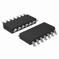
MC74ACT125DR2G ON Semiconductor, MC74ACT125DR2G Datasheet - Page 3

MC74ACT125DR2G
Manufacturer Part Number
MC74ACT125DR2G
Description
IC BUFF TRI-ST QD N-INV 14SOIC
Manufacturer
ON Semiconductor
Series
74ACTr
Datasheet
1.MC74AC125DTR2G.pdf
(9 pages)
Specifications of MC74ACT125DR2G
Logic Type
Buffer/Line Driver, Non-Inverting
Number Of Elements
4
Number Of Bits Per Element
1
Current - Output High, Low
24mA, 24mA
Voltage - Supply
4.5 V ~ 5.5 V
Operating Temperature
-40°C ~ 85°C
Mounting Type
Surface Mount
Package / Case
14-SOIC (3.9mm Width), 14-SOL
Logic Family
74ACT
Number Of Channels Per Chip
Quad
Polarity
Non-Inverting
Supply Voltage (max)
5.5 V
Supply Voltage (min)
4.5 V
Maximum Operating Temperature
85 C
Mounting Style
SMD/SMT
High Level Output Current
- 24 mA
Input Bias Current (max)
8 uA
Low Level Output Current
24 mA
Maximum Power Dissipation
500 mW
Minimum Operating Temperature
- 40 C
Number Of Lines (input / Output)
3
Output Type
3-State
Propagation Delay Time
9 ns @ 5 V
Logical Function
Buffer/Line Driver
Number Of Elements
4
Number Of Channels
4
Number Of Inputs
4
Number Of Outputs
4
Operating Supply Voltage (typ)
5V
Package Type
SOIC
Operating Supply Voltage (max)
5.5V
Operating Supply Voltage (min)
4.5V
Quiescent Current
8uA
Technology
CMOS
Pin Count
14
Mounting
Surface Mount
Operating Temp Range
-40C to 85C
Operating Temperature Classification
Industrial
Lead Free Status / RoHS Status
Lead free / RoHS Compliant
Other names
MC74ACT125DR2GOS
MC74ACT125DR2GOS
MC74ACT125DR2GOSTR
MC74ACT125DR2GOS
MC74ACT125DR2GOSTR
Available stocks
Company
Part Number
Manufacturer
Quantity
Price
Part Number:
MC74ACT125DR2G
Manufacturer:
ON/安森美
Quantity:
20 000
DC CHARACTERISTICS
Symbol
*All outputs loaded; thresholds on input associated with output under test.
†Maximum test duration 2.0 ms, one input loaded at a time.
NOTE:
AC CHARACTERISTICS
Symbol
*Voltage Range 3.3 V is 3.3 V ±0.3 V.
Voltage Range 5.0 V is 5.0 V ±0.5 V.
I
V
I
t
t
t
t
V
t
t
V
I
OHD
I
V
OLD
PLH
PHL
PZH
PHZ
PZL
PLZ
I
OZ
CC
OH
IN
OL
IH
IL
I
IN
Minimum High Level
Input Voltage
Maximum Low Level
Input Voltage
Minimum High Level
Output Voltage
Minimum Low Level
Output Voltage
Maximum Input
Leakage Current
V
V
V
†Minimum Dynamic
Maximum Quiescent
Supply Current
Propagation Delay
Data to Output
Propagation Delay
Data to Output
Output Enable
Time
Output Enable
Time
Output Disable
Time
Output Disable
Time
Output Current
I
I
O
and I
(OE) = V
= V
= V
CC
CC
CC
, GND
@ 3.0 V are guaranteed to be less than or equal to the respective limit @ 5.5 V.
, GND
IL
, V
IH
Parameter
Parameter
http://onsemi.com
V
(V)
3.0
4.5
5.5
3.0
4.5
5.5
3.0
4.5
5.5
3.0
4.5
5.5
3.0
4.5
5.5
3.0
4.5
5.5
5.5
5.5
5.5
5.5
5.5
CC
3
0.002
0.001
0.001
2.25
2.75
2.25
2.75
2.99
4.46
5.49
Typ
T
1.5
1.5
−
−
−
−
−
−
−
−
−
−
−
A
74AC
= +25°C
3.15
3.85
1.35
1.65
2.56
3.86
4.86
0.36
0.36
0.36
±0.1
±0.5
Guaranteed Limits
2.1
0.9
2.9
4.4
5.4
0.1
0.1
0.1
8.0
−
−
V
(V)
3.3
5.0
3.3
5.0
3.3
5.0
3.3
5.0
3.3
5.0
3.3
5.0
CC
−40°C to
*
74AC
+85°C
T
3.15
3.85
1.35
1.65
2.46
3.76
4.76
0.44
0.44
0.44
±1.0
±5.0
−75
2.1
0.9
2.9
4.4
5.4
0.1
0.1
0.1
75
80
A
=
Min
T
1.0
1.0
1.0
1.0
1.0
1.0
1.0
1.0
1.0
1.0
1.0
1.0
C
A
L
74AC
= +25°C
= 50 pF
Max
10.5
10.5
9.0
7.0
9.0
7.0
7.0
8.0
9.0
9.0
Unit
10
10
mA
mA
mA
mA
mA
V
V
V
V
V
V
Min
T
C
1.0
1.0
1.0
1.0
1.0
1.0
1.0
1.0
1.0
1.0
1.0
1.0
V
or V
V
or V
I
*V
I
I
*V
I
V
V
V
V
V
V
V
OUT
OH
OUT
OL
A
to +85°C
OUT
OUT
I
I
I
O
OLD
OHD
IN
L
IN
IN
(OE) = V
= V
= V
74AC
= −40°C
= 50 pF
= V
= V
CC
CC
= V
= V
= − 50 mA
= 50 mA
= 0.1 V
= 0.1 V
CC
= 1.65 V Max
CC
Conditions
= 3.85 V Min
CC
− 0.1 V
− 0.1 V
CC
Max
10.5
11.5
7.5
7.5
8.0
8.5
9.5
9.5
IL
IL
10
10
11
11
, GND
, GND
, GND
or V
−12 mA
− 24 mA
− 24 mA
or V
12 mA
24 mA
24 mA
or GND
IL
, V
IH
IH
IH
Unit
ns
ns
ns
ns
ns
ns


