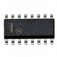
MC74HC4020ADG ON Semiconductor, MC74HC4020ADG Datasheet - Page 6

MC74HC4020ADG
Manufacturer Part Number
MC74HC4020ADG
Description
IC COUNTER 14STAGE BIN 16-SOIC
Manufacturer
ON Semiconductor
Series
74HCr
Datasheet
1.MC74HC4020ADR2G.pdf
(12 pages)
Specifications of MC74HC4020ADG
Logic Type
Binary Counter
Direction
Up
Number Of Elements
1
Number Of Bits Per Element
14
Reset
Asynchronous
Count Rate
50MHz
Trigger Type
Negative Edge
Voltage - Supply
2 V ~ 6 V
Operating Temperature
-55°C ~ 125°C
Mounting Type
Surface Mount
Package / Case
16-SOIC (3.9mm Width)
Counter Type
Binary
Counting Sequence
Up
Number Of Circuits
1
Logic Family
74HC
Propagation Delay Time
96 ns, 63 ns, 31 ns, 25 ns
Supply Voltage (max)
6 V
Maximum Operating Temperature
+ 125 C
Minimum Operating Temperature
- 55 C
Function
Counter
Mounting Style
SMD/SMT
Operating Supply Voltage
2 V to 6 V
Rohs Compliant
YES
Timing
-
Clock Frequency
50MHz
Count Maximum
16383
Supply Voltage Range
2V To 6V
Logic Case Style
SOIC
No. Of Pins
16
Operating Temperature Range
-55°C To +125°C
Lead Free Status / RoHS Status
Lead free / RoHS Compliant
Timing
-
Lead Free Status / Rohs Status
Lead free / RoHS Compliant
Available stocks
Company
Part Number
Manufacturer
Quantity
Price
Company:
Part Number:
MC74HC4020ADG
Manufacturer:
ON Semiconductor
Quantity:
1 916
NOTE: Information on typical parametric values can be found in Chapter 2 of the ON Semiconductor High−Speed CMOS Data Book
INPUTS
Clock (Pin 10)
transition on this input advances the state of the counter.
Reset (Pin 11)
asynchronously resets the counter to its zero state, thus
forcing all Q outputs low.
TIMING REQUIREMENTS
Symbol
Negative−edge triggering clock input. A high−to−low
Active−high reset. A high level applied to this input
Clock
t
t
r
rec
t
t
, t
w
w
Q1
f
(DL129/D).
10%
Minimum Recovery Time, Reset Inactive to Clock
(Figure 2)
Minimum Pulse Width, Clock
(Figure 1)
Minimum Pulse Width, Reset
(Figure 2)
Maximum Input Rise and Fall Times
(Figure 1)
50%
90%
90%
50%
10%
t
f
t
t
PLH
w
t
TLH
Figure 3.
1/f
(Input t
MAX
t
r
r
= t
t
PHL
f
= 6 ns)
Parameter
t
THL
SWITCHING WAVEFORMS
PIN DESCRIPTIONS
V
GND
http://onsemi.com
CC
6
OUTPUTS
Q1, Q4—Q14 (Pins 9, 7, 5, 4, 6, 13, 12, 14, 15, 1, 2, 3)
input frequency by 2
Active−high outputs. Each Qn output divides the Clock
Any Q
Reset
Clock
V
2.0
3.0
4.5
6.0
2.0
3.0
4.5
6.0
2.0
3.0
4.5
6.0
2.0
3.0
4.5
6.0
V
CC
N
−55 to 25°C
.
1000
800
500
400
Figure 4.
30
20
70
40
15
13
70
40
15
13
5
4
Guaranteed Limit
t
PHL
50%
≤85°C
t
1000
w
800
500
400
40
25
80
45
19
16
80
45
19
16
t
8
6
rec
50%
50%
≤125°C
1000
800
500
400
50
30
12
90
50
24
20
90
50
24
20
9
V
GND
V
GND
Unit
CC
CC
ns
ns
ns
ns


