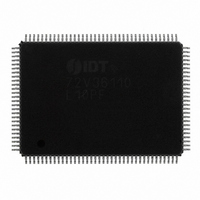
IDT72V36110L10PF IDT, Integrated Device Technology Inc, IDT72V36110L10PF Datasheet - Page 4

IDT72V36110L10PF
Manufacturer Part Number
IDT72V36110L10PF
Description
IC FIFO SYNC 131KX36 10NS 128QFP
Manufacturer
IDT, Integrated Device Technology Inc
Series
72Vr
Datasheet
1.IDT72V36110L7-5BB.pdf
(48 pages)
Specifications of IDT72V36110L10PF
Function
Synchronous
Memory Size
4.7M (131K x 36)
Data Rate
166MHz
Access Time
10ns
Voltage - Supply
3.15 V ~ 3.45 V
Operating Temperature
0°C ~ 70°C
Mounting Type
Surface Mount
Package / Case
128-TQFP, 128-VQFP
Configuration
Dual
Density
4.5Mb
Access Time (max)
6.5ns
Word Size
36b
Organization
128Kx36
Sync/async
Synchronous
Expandable
Yes
Bus Direction
Uni-Directional
Package Type
TQFP
Clock Freq (max)
100MHz
Operating Supply Voltage (typ)
3.3V
Operating Supply Voltage (min)
3.15V
Operating Supply Voltage (max)
3.45V
Supply Current
40mA
Operating Temp Range
0C to 70C
Operating Temperature Classification
Commercial
Mounting
Surface Mount
Pin Count
128
Lead Free Status / RoHS Status
Contains lead / RoHS non-compliant
Other names
72V36110L10PF
800-1530
800-1530
Available stocks
Company
Part Number
Manufacturer
Quantity
Price
Company:
Part Number:
IDT72V36110L10PF
Manufacturer:
IDT, Integrated Device Technology Inc
Quantity:
10 000
Part Number:
IDT72V36110L10PF
Manufacturer:
IDT
Quantity:
20 000
Company:
Part Number:
IDT72V36110L10PF8
Manufacturer:
IDT, Integrated Device Technology Inc
Quantity:
10 000
DESCRIPTION (CONTINUED)
operation, which consists of activating REN and enabling a rising RCLK edge,
will shift the word from internal memory to the data output lines.
to the data output lines after three transitions of the RCLK signal. A REN does
not have to be asserted for accessing the first word. However, subsequent
words written to the FIFO do require a LOW on REN for access. The state of
the FWFT/SI input during Master Reset determines the timing mode in use.
can provide, the FWFT timing mode permits depth expansion by chaining FIFOs
in series (i.e. the data outputs of one FIFO are connected to the corresponding
data inputs of the next). No external logic is required.
FF/IR (Full Flag or Input Ready), HF (Half-full Flag), PAE (Programmable
Almost-Empty flag) and PAF (Programmable Almost-Full flag). The EF and FF
functions are selected in IDT Standard mode. The IR and OR functions are
selected in FWFT mode. HF, PAE and PAF are always available for use,
irrespective of timing mode.
memory. Programmable offsets determine the flag switching threshold and can
be loaded by two methods: parallel or serial. Eight default offset settings are also
provided, so that PAE can be set to switch at a predefined number of locations
IDT72V36100/72V36110 3.3V HIGH DENSITY SUPERSYNC II
65,536 x 36 and 131,072 x 36
In FWFT mode, the first word written to an empty FIFO is clocked directly
For applications requiring more data storage capacity than a single FIFO
PAE and PAF can be programmed independently to switch at any point in
These FIFOs have five flag pins, EF/OR (Empty Flag or Output Ready),
PROGRAMMABLE ALMOST-FULL (PAF)
FULL FLAG/INPUT READY (FF/IR)
(x36, x18 or x9) DATA IN (D
FIRST WORD FALL THROUGH/
WRITE CLOCK (WCLK/WR*)
SERIAL INPUT (FWFT/SI)
WRITE ENABLE (WEN)
SERIAL ENABLE(SEN)
Figure 1. Single Device Configuration Signal Flow Diagram
PARTIAL RESET (PRS)
INPUT WIDTH (IW)
LOAD (LD)
0
- D
TM
n
)
36-BIT FIFO
MATCHING
72V36100
72V36110
BUS-
(BM)
4
IDT
from the empty boundary and the PAF threshold can also be set at similar
predefined values from the full boundary. The default offset values are set during
Master Reset by the state of the FSEL0, FSEL1, and LD pins.
WCLK, are used to load the offset registers via the Serial Input (SI). For parallel
programming, WEN together with LD on each rising edge of WCLK, are used
to load the offset registers via D
of RCLK can be used to read the offsets in parallel from Q
serial or parallel offset loading has been selected.
pointers are set to the first location of the FIFO. The FWFT pin selects IDT
Standard mode or FWFT mode.
location of the memory. However, the timing mode, programmable flag
programming method, and default or programmed offset settings existing before
Partial Reset remain unchanged. The flags are updated according to the timing
mode and offsets in effect. PRS is useful for resetting a device in mid-operation,
when reprogramming programmable flags would be undesirable.
Empty flag) and PAF (Programmable Almost-Full flag) outputs. The timing
modes can be set to be either asynchronous or synchronous for the PAE and
PAF flags.
MASTER RESET (MRS)
For serial programming, SEN together with LD on each rising edge of
During Master Reset (MRS) the following events occur: the read and write
The Partial Reset (PRS) also sets the read and write pointers to the first
It is also possible to select the timing mode of the PAE (Programmable Almost-
OUTPUT WIDTH (OW)
RETRANSMIT (RT)
PROGRAMMABLE ALMOST-EMPTY (PAE)
READ CLOCK (RCLK/RD*)
READ ENABLE (REN)
EMPTY FLAG/OUTPUT READY (EF/OR)
HALF-FULL FLAG (HF)
BIG-ENDIAN/LITTLE-ENDIAN (BE)
INTERSPERSED/
NON-INTERSPERSED PARITY (IP)
(x36, x18 or x9) DATA OUT (Q
OUTPUT ENABLE (OE)
n
. REN together with LD on each rising edge
COMMERCIAL AND INDUSTRIAL
TEMPERATURE RANGES
0
OCTOBER 22, 2008
n
- Q
regardless of whether
n
)
6117 drw03


