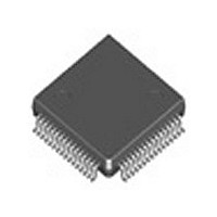
IDT72V851L10TF IDT, Integrated Device Technology Inc, IDT72V851L10TF Datasheet - Page 15

IDT72V851L10TF
Manufacturer Part Number
IDT72V851L10TF
Description
IC FIFO SYNC 4096X18 10NS 64QFP
Manufacturer
IDT, Integrated Device Technology Inc
Series
72Vr
Datasheet
1.IDT72V841L15PFG.pdf
(16 pages)
Specifications of IDT72V851L10TF
Function
Asynchronous
Memory Size
72K (4K x 18)
Data Rate
100MHz
Access Time
10ns
Voltage - Supply
3 V ~ 3.6 V
Operating Temperature
0°C ~ 70°C
Mounting Type
Surface Mount
Package / Case
64-STQFP
Configuration
Quad
Density
144Kb
Access Time (max)
6.5ns
Word Size
9b
Organization
8Kx9x2
Sync/async
Synchronous
Expandable
Yes
Bus Direction
Bi-Directional
Package Type
STQFP
Clock Freq (max)
100MHz
Operating Supply Voltage (typ)
3.3V
Operating Supply Voltage (min)
3V
Operating Supply Voltage (max)
3.6V
Supply Current
40mA
Operating Temp Range
0C to 70C
Operating Temperature Classification
Commercial
Mounting
Surface Mount
Pin Count
64
Lead Free Status / RoHS Status
Contains lead / RoHS non-compliant
Other names
72V851L10TF
Available stocks
Company
Part Number
Manufacturer
Quantity
Price
Company:
Part Number:
IDT72V851L10TF
Manufacturer:
IDT, Integrated Device Technology Inc
Quantity:
10 000
Company:
Part Number:
IDT72V851L10TF8
Manufacturer:
IDT, Integrated Device Technology Inc
Quantity:
10 000
Company:
Part Number:
IDT72V851L10TFG
Manufacturer:
IDT, Integrated Device Technology Inc
Quantity:
10 000
TWO PRIORITY DATA BUFFER
CONFIGURATION
72V841/72V851 can be used to prioritize two different types of data shared
on a system bus. When writing from the bus to the FIFO, control logic sorts
BIDIRECTIONAL CONFIGURATION
72V851 can be used to buffer data flow in two directions. In the example that
IDT72V801/72V8211/72V821/72V831/72V841/72V851 3.3V DUAL CMOS SyncFIFO
DUAL 256 x 9, DUAL 512 x 9, DUAL 1K x 9, DUAL 2K x 9, DUAL 4K x 9, DUAL 8K x 9
The two FIFOs contained in the IDT72V801/72V811/72V821/72V831/
The two FIFOs of the IDT72V801/72V811/72V821/72V831/72V841/
Processor
Processor
RAM
RAM
Address
Address
Control
Control
Clock
Clock
Data
Data
9
9
9
9
Figure 17. Block Diagram of Bidirectional Configuration
Figure 16. Block Diagram of Two Priority Configuration
V
CC
9
V
CC
9
9
9
RCLKB
OEB
WENA2 RENA2
WCLKA
WENA1
DA0-DA8
RAM ARRAY B
RENB1
RENB2
QB0-QB8
RAM ARRAY A
WCLKB
72V801
72V811
72V821
72V831
72V841
72V851
D
WENB1
D
WCLKA
WENA1
WENA2 RENA2
WENB2 RENB2
RAM ARRAY B
RAM ARRAY A
QA0-QA8
A0
B0
IDT
DB0-DB8
V
WENB1
WCLKB
WENB2
RENA1
-D
-D
RCLKA
CC
72V801
72V811
72V821
72V831
72V841
72V851
V
A8
B8
OEA
CC
IDT
15
Q
Q
A0
RCLKB
RCLKA
RENB1
B0
the intermixed data according to type, sending one kind to FIFO A and the other
kind to FIFO B. Then, at the outputs, each data type is transferred to its
appropriate destination. Additional IDT72V801/72V811/72V821/72V831/
72V841/72V851s permit more than two priority levels. Priority buffering is
particularly useful in network applications.
RENA
follows, a processor can write data to a peripheral controller via FIFO A, and,
in turn, the peripheral controller can write the processor via FIFO B.
OEB2
-Q
-Q
OEA
A8
B8
9
9
TM
9
9
Clock
Data
Clock
Data
9
Processing
Processing
Image
Voice
Card
Card
DMA Clock
Control
Address
Data
Peripheral
Control
Controller
Control
Address
Address
COMMERCIAL AND INDUSTRIAL
TEMPERATURE RANGES
I/O Data
4093 drw 19
OCTOBER 22, 2008
4093 drw 18
I/O Data
I/O Data


