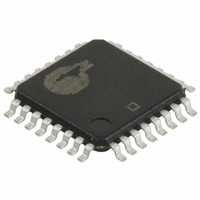
CY7C4251-15AC Cypress Semiconductor Corp, CY7C4251-15AC Datasheet

CY7C4251-15AC
Specifications of CY7C4251-15AC
Available stocks
Related parts for CY7C4251-15AC
CY7C4251-15AC Summary of contents
Page 1
... High-speed 100-MHz operation (10 ns Read/Write cycle time) • Low power ( mA) CC • Fully asynchronous and simultaneous Read and Write operation • ...
Page 2
... In this configuration, WEN2/LD can be used to access the four 8-bit offset registers contained in the CY7C42X1 for writing or reading data to these registers. CY7C4231/4241/4251 -25 Unit 40 MHz ICC1 40 CY7C4241 CY7C4251 4K × × 9 before RCLK for it ENS ENS 0–8 outputs 0–8 outputs 0–8 Page ...
Page 3
When the device is configured for programmable flags and both WEN2/LD and WEN1 are LOW, the first LOW-to-HIGH transition of WCLK writes data from the data inputs to the empty offset least significant bit (LSB) register. The second, third, and ...
Page 4
... Full Offset ( default value). Document #: 38-06016 Rev. *B (256 – m), CY7C4211 (512 – m), CY7C4221 (1K – m), CY7C4231 (2K – m), CY7C4241 (4K – m), and CY7C4251 (8K – m). PAF is set HIGH by the LOW-to-HIGH transition of WCLK when the number of available memory locations is greater than m. Table 1. Writing the Offset Registers ...
Page 5
Width Expansion Configuration Word width may be increased simply by connecting the corre- sponding input controls signals of multiple devices. A composite flag should be created for each of the end-point status flags (EF and FF). The partial status flags ...
Page 6
Maximum Ratings (Above which the useful life may be impaired. For user guide- lines, not tested.) Storage Temperature ...................................–65 Ambient Temperature with Power Applied...............................................–55 Supply Voltage to Ground Potential ............... –0.5V to +7.0V DC Voltage Applied to Outputs in ...
Page 7
Electrical Characteristics Over the Operating Range Parameter Description V Output HIGH Voltage OH V Output LOW Voltage OL V Input HIGH Voltage IH V Input LOW Voltage IL I Input Leakage IX Current [7] I Output Short OS Circuit Current ...
Page 8
Switching Characteristics Over the Operating Range Parameter Description t Data Hold Time DH t Enable Set-up Time ENS t Enable Hold Time ENH [13] t Reset Pulse Width RS t Reset Set-up Time RSS t Reset Recovery Time RSR t ...
Page 9
Switching Waveforms (continued) Read Cycle Timing RCLK t t ENS REN1,REN2 EF Q – OLZ OE WCLK WEN1 WEN2 [17] Reset Timing RS REN1, REN2 WEN1 [18] WEN2/LD EF,PAE FF,PAF Notes: 15. ...
Page 10
Switching Waveforms (continued) First Data Word Latency after Reset with Simultaneous Read and Write WCLK – (FIRST ENS WEN1 WEN2 (if applicable) RCLK EF REN1, REN2 Q – Empty ...
Page 11
Switching Waveforms (continued) Full Flag Timing NO Write WCLK [15] t SKEW1 D – WEN1 WEN2 (if applicable) RCLK t ENS REN1, REN2 LOW OE Q –Q DATA IN OUTPUT REGISTER 0 8 Programmable Almost Empty Flag ...
Page 12
... PAF offset = m. 27. 64-m words for CY7C4421, 256 – m words in FIFO for CY7C4201, 512 – m words for CY7C4211, 1024 – m words for CY7C4221, 2048 – m words for CY7C4231, 4096 – m words for CY7C4241, 8192 – m words for CY7C4251. 28 the minimum time between a rising RCLK edge and a rising WCLK edge for PAF to change during that clock cycle. If the time between the rising ...
Page 13
Switching Waveforms (continued) Read Programmable Registers t CLK t CLKH RCLK t ENS WEN2/LD t ENS REN1, REN2 Q – Document #: 38-06016 Rev. *B CY7C4421/4201/4211/4221 t CLKL t ENH t A UNKNOWN PAE OFFSET LSB CY7C4231/4241/4251 PAF ...
Page 14
Typical AC and DC Characteristics NORMALIZED SUPPLY CURRENT vs. SUPPLY VOLTAGE 1.4 1 100 MHz 0.6 4 4.5 5 5.5 6 SUPPLY VOLTAGE (V) NORMALIZED t vs. ...
Page 15
Ordering Information Synchronous FIFO Speed (ns) Ordering Code 10 CY7C4421-10AC CY7C4421-10JC 15 CY7C4421-15AC CY7C4421-15JC 256 x 9 Synchronous FIFO Speed (ns) Ordering Code 10 CY7C4201-10AC CY7C4201-10JC 15 CY7C4201-15AC CY7C4201-15JC 25 CY7C4201-25AC CY7C4201-25JC CY7C4201-25AI 512 x 9 Synchronous ...
Page 16
... CY7C4241-10JI 15 CY7C4241-15AC CY7C4241-15JC 25 CY7C4241-25AC CY7C4241-25JC CY7C4241-25JI Synchronous FIFO Speed (ns) Ordering Code 10 CY7C4251-10AC CY7C4251-10JC CY7C4251-10AI 15 CY7C4251-15AC CY7C4251-15JC 25 CY7C4251-25AC CY7C4251-25JC CY7C4251-25AI Document #: 38-06016 Rev. *B CY7C4421/4201/4211/4221 Package Package Name Type J65 32-lead Plastic Leaded Chip Carrier A32 32-lead Thin Quad Flatpack J65 32-lead Plastic Leaded Chip Carrier ...
Page 17
... Document #: 38-06016 Rev. *B © Cypress Semiconductor Corporation, 2002. The information contained herein is subject to change without notice. Cypress Semiconductor Corporation assumes no responsibility for the use of any circuitry other than circuitry embodied in a Cypress Semiconductor product. Nor does it convey or imply any license under patent or other rights. Cypress Semiconductor does not authorize its products for use as critical components in life-support systems where a malfunction or failure may reasonably be expected to result in significant injury to the user ...
Page 18
Document Title: CY7C4421/4201/4211/4221, CY7C4231/4241/4251 64/256/512/1K/2K/4K/ Synchronous FIFOs Document Number: 38-06016 Issue REV. ECN NO. Date ** 106477 09/10/01 *A 110725 03/20/02 *B 122268 12/26/02 Document #: 38-06016 Rev. *B Orig. of Change Description of Change SZV Change from ...


