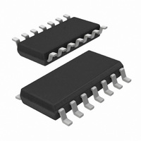
74LVC08AD,118 NXP Semiconductors, 74LVC08AD,118 Datasheet - Page 6

74LVC08AD,118
Manufacturer Part Number
74LVC08AD,118
Description
IC GATE AND QUAD 2-IN 14-SOIC
Manufacturer
NXP Semiconductors
Series
74LVCr
Datasheet
1.74LVC08AD118.pdf
(20 pages)
Specifications of 74LVC08AD,118
Number Of Circuits
4
Package / Case
14-SOIC (3.9mm Width), 14-SOL
Logic Type
AND Gate
Number Of Inputs
2
Current - Output High, Low
24mA, 24mA
Voltage - Supply
1.2 V ~ 3.6 V
Operating Temperature
-40°C ~ 125°C
Mounting Type
Surface Mount
Product
AND
Logic Family
74LVC
High Level Output Current
- 24 mA
Low Level Output Current
24 mA
Propagation Delay Time
11 ns
Supply Voltage (max)
3.6 V
Supply Voltage (min)
1.2 V
Maximum Operating Temperature
+ 125 C
Mounting Style
SMD/SMT
Minimum Operating Temperature
- 40 C
Logical Function
AND
Number Of Elements
4
Operating Supply Voltage (typ)
1.8/2.5/3.3V
Operating Temp Range
-40C to 125C
Package Type
SO
Number Of Outputs
1
Technology
CMOS
Mounting
Surface Mount
Pin Count
14
Operating Temperature Classification
Automotive
Quiescent Current
40uA
Operating Supply Voltage (max)
3.6V
Operating Supply Voltage (min)
1.2V
Lead Free Status / RoHS Status
Lead free / RoHS Compliant
Lead Free Status / RoHS Status
Lead free / RoHS Compliant, Lead free / RoHS Compliant
Other names
568-2273-2
74LVC08AD-T
935250020118
74LVC08AD-T
935250020118
Philips Semiconductors
RECOMMENDED OPERATING CONDITIONS
LIMITING VALUES
In accordance with the Absolute Maximum Rating System (IEC 60134); voltages are referenced to GND (ground = 0 V).
Notes
1. The input and output voltage ratings may be exceeded if the input and output current ratings are observed.
2. For SO14 packages: above 70 C derate linearly with 8 mW/K.
2003 Feb 24
V
V
V
T
t
V
I
V
I
V
I
I
T
P
SYMBOL
SYMBOL
r
IK
OK
O
CC
, t
amb
stg
CC
I
O
CC
I
O
tot
Quad 2-input AND gate
f
, I
For SSOP14 and TSSOP14 packages: above 60 C derate linearly with 5.5 mW/K.
For DHVQFN14 packages: above 60 C derate linearly with 4.5 mW/K.
GND
supply voltage
input voltage
output voltage
operating ambient temperature
input rise and fall times
supply voltage
input diode current
input voltage
output diode current
output voltage
output source or sink current
V
storage temperature
power dissipation
CC
or GND current
PARAMETER
PARAMETER
for maximum speed performance
for low-voltage applications
V
V
V
note 1
V
note 1
V
T
amb
CC
CC
I
O
O
< 0
> V
= 0 to V
= 1.2 to 2.7 V
= 2.7 to 3.6 V
=
CC
40 to +125 C; note 2
CONDITIONS
CONDITIONS
or V
6
CC
O
< 0
2.7
1.2
0
0
0
0
40
0.5
0.5
0.5
65
MIN.
MIN.
3.6
3.6
5.5
V
+125
20
10
+6.5
+6.5
V
+150
500
50
50
50
100
CC
CC
Product specification
MAX.
MAX.
74LVC08A
+ 0.5 V
V
V
V
V
ns/V
ns/V
V
mA
V
mA
mA
mA
mW
C
C
UNIT
UNIT


