74AHCT594DB,118 NXP Semiconductors, 74AHCT594DB,118 Datasheet
74AHCT594DB,118
Specifications of 74AHCT594DB,118
74AHCT594DB-T
935282015118


Related parts for 74AHCT594DB,118


74AHCT594DB,118 Summary of contents
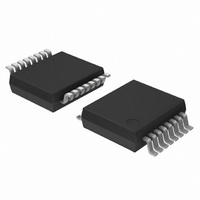
Page 1
Rev. 02 — 9 June 2008 1. General description The 74AHC594; 74AHCT594 is a high-speed Si-gate CMOS device and is pin compatible with Low-Power Schottky TTL (LSTTL specified in compliance ...
Page 2
... NXP Semiconductors 4. Ordering information Table 1. Ordering information Type number Package Temperature range Name 74AHC594 74AHC594D +125 C 74AHC594DB +125 C 74AHC594PW +125 C 74AHC594BQ +125 C 74AHCT594 74AHCT594D +125 C 74AHCT594DB +125 C 74AHCT594PW +125 C 74AHCT594BQ +125 C 5. Functional diagram Fig 1. Functional diagram 74AHC_AHCT594_2 Product data sheet ...
Page 3
... NXP Semiconductors SHCP STCP SHR STR Fig 2. Logic symbol DS SHCP SHR STCP STR Fig 4. Logic diagram 74AHC_AHCT594_2 Product data sheet 74AHC594; 74AHCT594 Q7S mbc319 Fig 3. STAGE 0 STAGES FFSH FFST Rev. 02 — 9 June 2008 8-bit shift register with output register 13 STR R2 12 ...
Page 4
... NXP Semiconductors 6. Pinning information 6.1 Pinning Fig 5. Pin configuration SO16 74AHC594 74AHCT594 GND 8 Fig 6. Pin configuration (T)SSOP16 74AHC_AHCT594_2 Product data sheet 74AHC594 74AHCT594 GND 8 001aae343 STR 12 STCP 11 SHCP 10 SHR 9 Q7S 001aae344 Fig 7. Rev. 02 — 9 June 2008 74AHC594; 74AHCT594 8-bit shift register with output register ...
Page 5
... NXP Semiconductors 6.2 Pin description Table 2. Pin description Symbol Pin GND 8 Q7S 9 SHR 10 SHCP 11 STCP 12 STR Functional description [1] Table 3. Function table Input SHCP STCP SHR STR [ HIGH voltage state LOW voltage state; = LOW to HIGH transition don’t care change; 74AHC_AHCT594_2 Product data sheet 74AHC594 ...
Page 6
... NXP Semiconductors SHCP DS STCP SHR STR Q7S Fig 8. Timing diagram 8. Limiting values Table 4. Limiting values In accordance with the Absolute Maximum Rating System (IEC 60134). Voltages are referenced to GND (ground = 0 V). Symbol Parameter V supply voltage CC V input voltage I I input clamping current ...
Page 7
... NXP Semiconductors 9. Recommended operating conditions Table 5. Operating conditions Symbol Parameter 74AHC594 V supply voltage CC V input voltage I V output voltage O T ambient temperature amb t/ V input transition rise and fall rate 74AHCT594 V supply voltage CC V input voltage I V output voltage O T ambient temperature ...
Page 8
... NXP Semiconductors Table 6. Static characteristics At recommended operating conditions; voltages are referenced to GND (ground = 0 V). Symbol Parameter Conditions I input leakage GND current 5 supply current 5 input capacitance 74AHCT594 V HIGH-level input voltage V LOW-level input voltage V HIGH-level output voltage 8.0 mA LOW-level output voltage ...
Page 9
... NXP Semiconductors Table 7. Dynamic characteristics Voltages are referenced to GND (ground = 0 V); for test circuit see Symbol Parameter Conditions STCP to Qn; see HIGH to LOW SHCP to Q7S; see PHL propagation delay 4 5 STCP to Qn; see SHR to Q7S; see ...
Page 10
... NXP Semiconductors Table 7. Dynamic characteristics Voltages are referenced to GND (ground = 0 V); for test circuit see Symbol Parameter Conditions t pulse width SHCP and STCP HIGH or W LOW; see SHR and STR HIGH or LOW; see Figure set-up time DS to SHCP; see ...
Page 11
... NXP Semiconductors Table 7. Dynamic characteristics Voltages are referenced to GND (ground = 0 V); for test circuit see Symbol Parameter Conditions t HIGH to LOW SHCP to Q7S; see PHL propagation delay STCP to Qn; see SHR to Q7S; see STR to Qn; see maximum SHCP or STCP; max frequency see ...
Page 12
... NXP Semiconductors 12. Waveforms Measurement points are given in Fig 9. Shift register clock pulse width, maximum frequency and input to output propagation delays SHCP input STCP input Q n outputs Measurement points are given in Fig 10. Shift register clock to storage register clock set-up time and storage clock pulse width, maximum ...
Page 13
... NXP Semiconductors SH CP input D S input Q 7 output Measurement points are given in The shaded areas indicate when the input is permitted to change for predictable output performance. Fig 11. Shift register clock to data input set-up and hold times Measurement points are given in Fig 12. Storage register reset pulse width, input to output propagation delay and recovery time ...
Page 14
... NXP Semiconductors Measurement points are given in Fig 13. Shift register reset pulse width, input to output propagation delay and recovery time Measurement points are given in Fig 14. Shift register reset to storage register clock set-up time Table 8. Measurement points Type 74AHC594 74AHCT594 74AHC_AHCT594_2 Product data sheet 74AHC594 ...
Page 15
... NXP Semiconductors For test data see Table 9. Definitions for test circuit Termination resistance should be equal to output impedance Load capacitance including jig and probe capacitance. L Fig 15. Load circuitry for measuring switching times Table 9. Test data Type Input V I 74AHC594 V CC 74AHCT594 3 ...
Page 16
... NXP Semiconductors 13. Package outline SO16: plastic small outline package; 16 leads; body width 3 pin 1 index 1 DIMENSIONS (inch dimensions are derived from the original mm dimensions) A UNIT max. 0.25 1.45 mm 1.75 0.25 0.10 1.25 0.010 0.057 inches 0.069 0.01 0.004 0.049 Note 1. Plastic or metal protrusions of 0.15 mm (0.006 inch) maximum per side are not included. ...
Page 17
... NXP Semiconductors SSOP16: plastic shrink small outline package; 16 leads; body width 5 pin 1 index 1 e DIMENSIONS (mm are the original dimensions) A UNIT max. 0.21 1. 0.25 0.05 1.65 Note 1. Plastic or metal protrusions of 0.25 mm maximum per side are not included. OUTLINE VERSION IEC SOT338-1 Fig 17. Package outline SOT338-1 (SSOP16) ...
Page 18
... NXP Semiconductors TSSOP16: plastic thin shrink small outline package; 16 leads; body width 4 pin 1 index 1 DIMENSIONS (mm are the original dimensions) A UNIT max. 0.15 0.95 mm 1.1 0.25 0.05 0.80 Notes 1. Plastic or metal protrusions of 0.15 mm maximum per side are not included. 2. Plastic interlead protrusions of 0.25 mm maximum per side are not included. ...
Page 19
... NXP Semiconductors DHVQFN16: plastic dual in-line compatible thermal enhanced very thin quad flat package; no leads; 16 terminals; body 2.5 x 3.5 x 0.85 mm terminal 1 index area terminal 1 index area DIMENSIONS (mm are the original dimensions) (1) A UNIT max. 0.05 0. 0.2 0.00 0.18 Note 1. Plastic or metal protrusions of 0.075 mm maximum per side are not included. ...
Page 20
... Document ID Release date 74AHC_AHCT594_2 20080609 • Modifications: The format of this data sheet has been redesigned to comply with the new identity guidelines of NXP Semiconductors. • Legal texts have been adapted to the new company name where appropriate. • Table 74AHC_AHCT594_1 20060704 74AHC_AHCT594_2 Product data sheet 74AHC594 ...
Page 21
... Right to make changes — NXP Semiconductors reserves the right to make changes to information published in this document, including without limitation specifications and product descriptions, at any time and without notice ...
Page 22
... NXP Semiconductors 18. Contents 1 General description . . . . . . . . . . . . . . . . . . . . . . 1 2 Features . . . . . . . . . . . . . . . . . . . . . . . . . . . . . . . 1 3 Applications . . . . . . . . . . . . . . . . . . . . . . . . . . . . 1 4 Ordering information . . . . . . . . . . . . . . . . . . . . . 2 5 Functional diagram . . . . . . . . . . . . . . . . . . . . . . 2 6 Pinning information . . . . . . . . . . . . . . . . . . . . . . 4 6.1 Pinning . . . . . . . . . . . . . . . . . . . . . . . . . . . . . . . 4 6.2 Pin description . . . . . . . . . . . . . . . . . . . . . . . . . 5 7 Functional description . . . . . . . . . . . . . . . . . . . 5 8 Limiting values Recommended operating conditions Static characteristics Dynamic characteristics . . . . . . . . . . . . . . . . . . 8 12 Waveforms . . . . . . . . . . . . . . . . . . . . . . . . . . . . 12 13 Package outline . . . . . . . . . . . . . . . . . . . . . . . . 16 14 Abbreviations ...