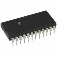
74F675APC Fairchild Semiconductor, 74F675APC Datasheet - Page 2

74F675APC
Manufacturer Part Number
74F675APC
Description
IC REG SER-IN SER-PAR OUT 24-DIP
Manufacturer
Fairchild Semiconductor
Series
74Fr
Datasheet
1.74F675APC.pdf
(6 pages)
Specifications of 74F675APC
Logic Type
Shift Register
Output Type
Standard
Number Of Elements
1
Number Of Bits Per Element
16
Function
Serial to Parallel, Serial
Voltage - Supply
4.5 V ~ 5.5 V
Operating Temperature
0°C ~ 70°C
Mounting Type
Through Hole
Package / Case
24-DIP (0.600", 15.24mm)
Lead Free Status / RoHS Status
Lead free / RoHS Compliant
Other names
74F675
Available stocks
Company
Part Number
Manufacturer
Quantity
Price
www.fairchildsemi.com
Unit Loading/Fan Out
Functional Description
The 16-Bit shift register operates in one of four modes, as
determined by the signals applied to the Chip Select (CS),
Read/Write (R/W) and Store Clock Pulse (STCP) input.
State changes are indicated by the falling edge of the Shift
Clock Pulse (SHCP). In the Shift Right mode, data enters
D
Serial Data Output (SO) pin. In the Parallel Load mode,
data from the storage register outputs enter the shift regis-
ter and serial shifting is inhibited.
Shift Register Operations Table
Logic Diagram
Please note that this diagram is provided only for the understanding of logic operations and should not be used to estimate propagation delays.
0
from the Serial Input (SI) pin and exits from Q
CS
H
L
L
L
Pin Names
SI
CS
SHCP
STCP
R/W
SO
Q
Control Inputs
0
–Q
R/W
H
H
X
L
15
SHCP STCP
X
Serial Data Input
Chip Select Input (Active LOW)
Shift Clock Pulse Input (Active Falling Edge)
Store Clock Pulse Input (Active Rising Edge)
Read/Write Input
Serial Data Output
Parallel Data Outputs
X
X
H
L
Hold
Shift Right
Shift Right
Parallel Load,
No Shifting
Operating
Mode
Description
15
via the
2
The storage register is in the Hold mode when either CS or
R/W is HIGH. With CS and R/W both LOW, the storage
register is parallel loaded from the shift register on the ris-
ing edge of STCP.
To prevent false clocking of the shift register, SHCP should
be in the LOW state during a LOW-to-HIGH transition of
CS. To prevent false clocking of the storage register, STCP
should be LOW during a HIGH-to-LOW transition of CS if
R/W is LOW, and should also be LOW during a HIGH-to-
LOW transition of R/W if CS is LOW.
Storage Register Operations Table
H
X
L
HIGH Voltage Level
LOW Voltage Level
Immaterial
HIGH-to-LOW Transition
LOW-to-HIGH Transition
CS
H
L
L
HIGH/LOW
Inputs
50/33.3
50/33.3
1.0/1.0
1.0/1.0
1.0/1.0
1.0/1.0
1.0/1.0
R/W
U.L.
X
H
L
STCP
X
X
Output I
20 A/ 0.6 mA
20 A/ 0.6 mA
20 A/ 0.6 mA
20 A/ 0.6 mA
20 A/ 0.6 mA
Input I
1 mA/20 mA
1 mA/20 mA
Hold
Hold
Parallel Load
Operating
Mode
IH
OH
/I
/I
IL
OL


