74F675APC Fairchild Semiconductor, 74F675APC Datasheet

IC REG SER-IN SER-PAR OUT 24-DIP

74F675APC

Manufacturer Part Number
74F675APC
Description
IC REG SER-IN SER-PAR OUT 24-DIP
Manufacturer
Fairchild Semiconductor
Series
74Fr
Datasheet

Specifications of 74F675APC

Logic Type
Shift Register
Output Type
Standard
Number Of Elements
1
Number Of Bits Per Element
16
Function
Serial to Parallel, Serial
Voltage - Supply
4.5 V ~ 5.5 V
Operating Temperature
0°C ~ 70°C
Mounting Type
Through Hole
Package / Case
24-DIP (0.600", 15.24mm)
Lead Free Status / RoHS Status
Lead free / RoHS Compliant
Other names
74F675

Available stocks

Company
Part Number
Manufacturer
Quantity
Price
Part Number:
74F675APC
Manufacturer:
FAI
Quantity:
13
© 1999 Fairchild Semiconductor Corporation
74F675ASC
74F675APC
74F675ASPC
74F675A
16-Bit Serial-In, Serial/Parallel-Out Shift Register
General Description
The 74F675A contains a 16-bit serial in/serial out shift reg-
ister and a 16-bit parallel out storage register. Separate
serial input and output pins are provided for expansion to
longer words. By means of a separate clock, the contents
of the shift register are transferred to the storage register.
The contents of the storage register can also be loaded
back into the shift register. A HIGH signal on the Chip
Select input prevents both shifting and parallel loading.
Ordering Code:
Devices also available in Tape and Reel. Specify by appending the suffix letter “X” to the ordering code.
Logic Symbols
Order Number
Package Number
IEEE/IEC
M24B
N24C
N24A
24-Lead Small Outline Integrated Circuit (SOIC), JEDEC MS-013, 0.300 Wide
24-Lead Plastic Dual-In-Line Package (PDIP), JEDEC MS-010, 0.600 Wide
24-Lead Plastic Dual-In-Line Package (PDIP), JEDEC MS-100, 0.300 Wide
DS009587
Features
Connection Diagram
Serial-to-parallel converter
16-Bit serial I/O shift register
16-Bit parallel out storage register
Recirculating parallel transfer
Expandable for longer words
Slim 24 lead package
74F675A version prevents false clocking through
CS or R/W inputs
Package Description
April 1988
Revised August 1999
www.fairchildsemi.com

Related parts for 74F675APC

74F675APC Summary of contents

Page 1

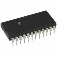
... Ordering Code: Order Number Package Number 74F675ASC M24B 24-Lead Small Outline Integrated Circuit (SOIC), JEDEC MS-013, 0.300 Wide 74F675APC N24A 24-Lead Plastic Dual-In-Line Package (PDIP), JEDEC MS-010, 0.600 Wide 74F675ASPC N24C 24-Lead Plastic Dual-In-Line Package (PDIP), JEDEC MS-100, 0.300 Wide Devices also available in Tape and Reel. Specify by appending the suffix letter “X” to the ordering code. ...

Page 2

Unit Loading/Fan Out Pin Names SI Serial Data Input Chip Select Input (Active LOW) CS Shift Clock Pulse Input (Active Falling Edge) SHCP STCP Store Clock Pulse Input (Active Rising Edge) Read/Write Input R/W SO Serial Data Output Q –Q ...

Page 3

Absolute Maximum Ratings Storage Temperature Ambient Temperature under Bias Junction Temperature under Bias V Pin Potential to Ground Pin CC Input Voltage (Note 2) Input Current (Note 5.0 mA Voltage Applied to Output in HIGH State ...

Page 4

AC Electrical Characteristics Symbol Parameter f Maximum Clock Frequency MAX t Propagation Delay PLH t STCP to Q PHL n t Propagation Delay PLH t SHCP to SO PHL AC Operating Requirements Symbol Parameter t (H) Setup Time, HIGH or ...

Page 5

Physical Dimensions inches (millimeters) unless otherwise noted 24-Lead Small Outline Integrated Circuit (SOIC), JEDEC MS-013, 0.300 Wide 24-Lead Plastic Dual-In-Line Package (PDIP), JEDEC MS-010, 0.600 Wide Package Number M24B Package Number N24A 5 www.fairchildsemi.com ...

Page 6

Physical Dimensions inches (millimeters) unless otherwise noted (Continued) 24-Lead Plastic Dual-In-Line Package (PDIP), JEDEC MS-100, 0.300 Wide Fairchild does not assume any responsibility for use of any circuitry described, no circuit patent licenses are implied and Fairchild reserves the right ...

Related keywords