NL7SZ18DFT2G ON Semiconductor, NL7SZ18DFT2G Datasheet
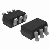
IC DEMUX 1:2 NONINV 3ST SC88

NL7SZ18DFT2G

Manufacturer Part Number
NL7SZ18DFT2G
Description
IC DEMUX 1:2 NONINV 3ST SC88
Manufacturer
ON Semiconductor
Series
7SZr
Type
Demultiplexerr
Datasheet

Specifications of NL7SZ18DFT2G

Circuit
1 x 1:2
Independent Circuits
1
Current - Output High, Low
32mA, 32mA
Voltage Supply Source
Single Supply
Voltage - Supply
1.65 V ~ 5.5 V
Operating Temperature
-40°C ~ 85°C
Mounting Type
Surface Mount
Package / Case
SC-70-6, SC-88, SOT-363
Lead Free Status / RoHS Status
Lead free / RoHS Compliant
Other names
NL7SZ18DFT2GOS

Available stocks

Company
Part Number
Manufacturer
Quantity
Price
Part Number:
NL7SZ18DFT2G
Manufacturer:
ON Semiconductor
Quantity:
2 300
Part Number:
NL7SZ18DFT2G
Manufacturer:
ON/安森美
Quantity:
20 000
Part Number:
NL7SZ18DFT2G
0
NL7SZ18
1-to-2 Demultiplexer with
3-State Deselected Output
demultiplexer. With the Select input [S] at Low, data at A is passed to
Y0 and Y1 is set to high impedance. With the Select input [S] at High,
data at A is passed to Y1 and Y0 is set to high impedance. The device
operates over the voltage range from 1.65 V to 5.5 V.
and offers mixed (1.65 V, 2.3 V, 3.0 V and 5.5 V) voltage capability by
providing over voltage tolerance (OVT*) circuitry on I/O pins.
Features
Typical Applications
Important Information
*Over Voltage Tolerance (OVT) enables input and output pins to function outside
© Semiconductor Components Industries, LLC, 2010
August, 2010 − Rev. 9
(higher) of their operating voltages, with no damage to the devices or to signal
integrity.
The NL7SZ18 is a high−performance non−inverting 1−to−2
This device has been optimized for on−board buffering applications
High−Speed Propagation Delay
Power Down Impedance
Output Drive Capability
Broad V
Surface Mount Technology
OVT* on Inputs/Outputs
Pb−Free Package is Available
Cell Phones
PDAs
Digital Cameras
Video Cameras
ESD Protection: MM >200 V, Human Body Model >2000 V
Latch−Up Max Rating: 300 mA
Pin−to−Pin Compatible with NC7SZ18
t
Outputs in High−Z
32 mA @ 5.0 V
1.65 V to 5.5 V
SC−70, 6−Lead and UDFN6 Packaging
PD
2.5 nS (Typ), Load 50 pF @ 5.0 V
Pin
Y
Y
A
S
CC
0
1
Operating Range
PIN/FUNCTION TABLE
Demultiplexer Select
Data Input
Function
Output 1
Output 2
1
See detailed ordering and shipping information in the package
dimensions section on page 2 of this data sheet.
SOT−363/SC70−6/SC−88
*Date Code orientation and/or position may vary
depending upon manufacturing location.
GND
H
H
S
L
L
(Note: Microdot may be in either location)
CASE 517AA
S
A
CASE 419B
MU SUFFIX
DF SUFFIX
Input
ORDERING INFORMATION
UDFN6
LD, T
M
G
1
1
2
3
1
http://onsemi.com
PIN ASSIGNMENT
TRUTH TABLE
A
H
H
L
L
(TOP VIEW)
= Device Marking
= Date Code*
= Pb−Free Package
MARKING DIAGRAMS
Publication Order Number:
1
Y
H
L
Z
Z
0
Output
T M
LD M G
G
6
5
4
G
NL7SZ18/D
Y
V
Y
0
CC
1
Y
Z
Z
H
L
1

Related parts for NL7SZ18DFT2G

NL7SZ18DFT2G Summary of contents

Page 1

NL7SZ18 1-to-2 Demultiplexer with 3-State Deselected Output The NL7SZ18 is a high−performance non−inverting 1−to−2 demultiplexer. With the Select input [S] at Low, data passed to Y0 and Y1 is set to high impedance. With the Select input ...

Page 2

... Output Voltage Operating Temperature Input Rise and Fall Times Thermal Resistance ORDERING INFORMATION Device Order Number NL7SZ18DFT2 NL7SZ18DFT2G NL7SZ18MUR2G †For information on tape and reel specifications, including part orientation and tape sizes, please refer to our Tape and Reel Packaging Specifications Brochure, BRD8011/D. Symbol V T ...

Page 3

DC ELECTRICAL CHARACTERISTICS Parameter Condition High−Level Input Voltage Low−Level Output Voltage High−Level −100 Output Voltage I = −4 −8 − ...

Page 4

AC ELECTRICAL CHARACTERISTICS Parameter Condition Propagation Delay 1 OPEN 500 OPEN ...

Page 5

A Input 10% t PLH 50% Output 90% S Input 50% 50% 10% t PZL Output 50% t PZH Output 50% Figure 3. AC Waveforms ...

Page 6

... 0.50 0.0197 0.40 0.0157 *For additional information on our Pb−Free strategy and soldering details, please download the ON Semiconductor Soldering and Mounting Techniques Reference Manual, SOLDERRM/D. PACKAGE DIMENSIONS SC−88/SC70−6/SOT−363 CASE 419B−02 ISSUE W NOTES: 1. DIMENSIONING AND TOLERANCING PER ANSI Y14.5M, 1982. ...

Page 7

... L 5X 0.40 PITCH *For additional information on our Pb−Free strategy and soldering details, please download the ON Semiconductor Soldering and Mounting Techniques Reference Manual, SOLDERRM/D. N. American Technical Support: 800−282−9855 Toll Free USA/Canada Europe, Middle East and Africa Technical Support: Phone: 421 33 790 2910 Japan Customer Focus Center Phone: 81− ...

Related keywords