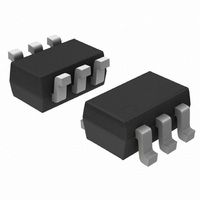
NL7SZ18DFT2G ON Semiconductor, NL7SZ18DFT2G Datasheet - Page 2

NL7SZ18DFT2G
Manufacturer Part Number
NL7SZ18DFT2G
Description
IC DEMUX 1:2 NONINV 3ST SC88
Manufacturer
ON Semiconductor
Series
7SZr
Type
Demultiplexerr
Datasheet
1.NL7SZ18DFT2G.pdf
(7 pages)
Specifications of NL7SZ18DFT2G
Circuit
1 x 1:2
Independent Circuits
1
Current - Output High, Low
32mA, 32mA
Voltage Supply Source
Single Supply
Voltage - Supply
1.65 V ~ 5.5 V
Operating Temperature
-40°C ~ 85°C
Mounting Type
Surface Mount
Package / Case
SC-70-6, SC-88, SOT-363
Lead Free Status / RoHS Status
Lead free / RoHS Compliant
Other names
NL7SZ18DFT2GOS
Available stocks
Company
Part Number
Manufacturer
Quantity
Price
Company:
Part Number:
NL7SZ18DFT2G
Manufacturer:
ON Semiconductor
Quantity:
2 300
Part Number:
NL7SZ18DFT2G
Manufacturer:
ON/安森美
Quantity:
20 000
Stresses exceeding Maximum Ratings may damage the device. Maximum Ratings are stress ratings only. Functional operation above the
Recommended Operating Conditions is not implied. Extended exposure to stresses above the Recommended Operating Conditions may affect
device reliability.
1. Measured with minimum pad spacing on an FR4 board, using 10 mm−by−1 inch, 2 ounce copper trace no air flow.
2. Tested to EIA/JESD22−A114−A.
3. Tested to EIA/JESD22−A115−A.
4. Tested to JESD22−C101−A.
†For information on tape and reel specifications, including part orientation and tape sizes, please refer to our Tape and Reel Packaging
RECOMMENDED OPERATING CONDITIONS
MAXIMUM RATINGS
ORDERING INFORMATION
Specifications Brochure, BRD8011/D.
DC Supply Voltage
DC Input Voltage
DC Output Voltage
DC Input Diode Current @ V
DC Output Diode Current @ V
DC Output Sink Current
DC Supply Current per Supply Pin
DC Ground Current per Ground Pin
Storage Temperature Range
Lead Temperature, 1 mm from Case for 10 Seconds
Junction Temperature Under Bias
Thermal Resistance (Note 1)
Power Dissipation in Still Air at 85°C
Moisture Sensitivity
Flammability Rating
ESD Withstand Voltage
DC Supply Voltage
DC Supply Voltage, Data Retention
Input Voltage
Output Voltage
Operating Temperature
Input Rise and Fall Times
Thermal Resistance
NL7SZ18DFT2
NL7SZ18DFT2G
NL7SZ18MUR2G
Device Order Number
1
t −0.5 V
1
t −0.5 V
Rating
Rating
Charged Device Model (Note 4)
Human Body Model (Note 2)
Machine Model (Note 3)
http://onsemi.com
Oxygen Index: 28 to 34
V
V
V
V
CC
CC
CC
CC
2
@ 1.8 " 0.15 V
(Pb−Free)
(Pb−Free)
Package
@ 2.5 " 0.2 V
@ 3.3 " 0.3 V
@ 5.0 " 0.5 V
SC70−6
SC70−6
UDFN6
Symbol
Symbol
V
T
V
V
I
I
MSL
V
V
V
GND
t
V
I
OUT
I
q
V
q
P
F
T
OUT
I
STG
T
T
ESD
OUT
r
OK
CC
CC
IK
CC
CC
, t
JA
JA
IN
IN
D
R
A
L
J
f
UL 94 V−0 @ 0125 in
3000 / Tape & Reel
3000 / Tape & Reel
3000 / Tape & Reel
Shipping
−0.5 to +7.0
−0.5 to +7.0
−0.5 to +7.0
−65 to +150
1.65 to 5.5
−55 to 125
1.5 to 5.5
0 to 5.5
0 to 5.5
Level 1
> 2000
0 to 20
0 to 20
0 to 10
Value
"100
"100
Value
> 200
0 to 5
+150
"50
−50
−50
260
250
180
350
n/a
†
°C/W
°C/W
nS/V
Unit
Unit
mW
mA
mA
mA
mA
mA
°C
°C
°C
°C
V
V
V
V
V
V
V
V
−
−


