IDT71V256SA12YG IDT, Integrated Device Technology Inc, IDT71V256SA12YG Datasheet - Page 2
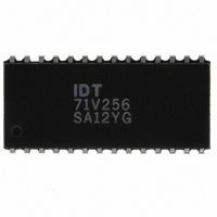
IDT71V256SA12YG
Manufacturer Part Number
IDT71V256SA12YG
Description
IC SRAM 256KBIT 12NS 28SOJ
Manufacturer
IDT, Integrated Device Technology Inc
Datasheet
1.IDT71V256SA15YG8.pdf
(8 pages)
Specifications of IDT71V256SA12YG
Format - Memory
RAM
Memory Type
SRAM
Memory Size
256K (32K x 8)
Speed
12ns
Interface
Parallel
Voltage - Supply
3 V ~ 3.6 V
Operating Temperature
0°C ~ 70°C
Package / Case
28-SOJ
Lead Free Status / RoHS Status
Lead free / RoHS Compliant
Other names
71V256SA12YG
800-1466
800-1466-5
800-1466
800-1466
800-1466-5
800-1466


Pin Configurations
Pin Descriptions
IDT71V256SA
3.3V CMOS Static RAM 256K (32K x 8-Bit)
V
A
A
A
A
WE
OE
CC
A
A
A
A
A
A
A
11
13
14
12
9
8
7
6
5
4
3
I/O
A
Name
0
GND
0
WE
V
CS
OE
- A
CC
- I/O
22
23
24
25
26
27
28
1
2
3
4
5
6
7
14
GND
7
I/O
I/O
I/O
A
A
A
A
A
A
A
A
A
A
14
12
7
6
5
4
3
2
1
0
0
1
2
Top View
Top View
1
2
3
4
5
6
7
8
9
10
11
12
13
14
DIP/SOJ
TSOP
SO28-5
SO28-8
28
27
26
25
24
23
22
21
20
19
18
17
16
15
Data Input/Output
Output Enable
Write Enable
Description
Chip Select
Addresses
Ground
Power
V
WE
A
A
A
A
OE
A
CS
I/O
I/O
I/O
I/O
I/O
3101 drw 02
CC
13
8
9
11
10
7
6
5
4
3
21
20
19
18
17
16
15
14
13
12
11
10
9
8
3101 drw 03
,
A
CS
I/O
I/O
I/O
I/O
I/O
GND
I/O
I/O
I/O
A
A
A
10
0
1
2
7
6
5
4
3
2
1
0
3101 tbl 01
,
2
Truth Table
Absolute Maximum Ratings
NOTES:
1. Stresses greater than those listed under ABSOLUTE MAXIMUM RATINGS
2. Input, Output, and I/O terminals; 4.6V maximum.
Capacitance
(T
NOTE:
1. This parameter is determined by device characterization, but is not production
Recommended Operating
Temperature and Supply Voltage
NOTE:
1. H = V
P
I
C
C
Commercial
Industrial
V
V
T
T
OUT
BIAS
STG
T
IN
OUT
CC
TERM
Symbol
A
may cause permanent damage to the device. This is a stress rating only and
functional operation of the device at these or any other conditions above those
indicated in the operational sections of this specification is not implied. Exposure
to absolute maximum rating conditions for extended periods may affect
reliability.
tested.
Symbol
WE
X
X
H
H
L
= +25°C, f = 1.0MHz, SOJ package)
(2)
Grade
IH
, L = V
Input Capacitance
Output Capacitance
V
CS
IL
Supply Voltage
Relative to GND
Relative to GND
Storage Temperature
Power Dissipation
DC Output Current
Terminal Voltage
Temperature Under Bias
H
L
L
L
HC
, X = Don’t Care
Commercial and Industrial Temperature Ranges
Parameter
(1)
-40
0
Temperature
O
Rating
C to +70
O
OE
X
X
X
C to +85
H
L
(1)
O
O
C
C
High-Z
High-Z
High-Z
D
D
I/O
OUT
V
Conditions
IN
V
OUT
IN
GND
= 3dV
0V
0V
= 3dV
-0.5 to V
-0.5 to +4.6
-55 to +125
-55 to +125
Standby (I
Standby (I
Output Disable
Read
Write
Com'l.
1.0
50
CC
Function
(1)
3.3V ± 0.3V
3.3V ± 0.3V
+0.5
Max.
SB
SB1
6
7
Vcc
)
)
3101 tbl 02
3101 tbl 03
3101 tbl 05
3101 tbl 04
Unit
mA
Unit
o
o
W
V
V
pF
pF
C
C
Related parts for IDT71V256SA12YG
Image
Part Number
Description
Manufacturer
Datasheet
Request
R

Part Number:
Description:
TRANSLATION DEVICE DPI 80-PQFP
Manufacturer:
IDT, Integrated Device Technology Inc
Datasheet:
Part Number:
Description:
IDT PART
Manufacturer:
IDT, Integrated Device Technology Inc
Datasheet:
Part Number:
Description:
IC LIU T1/E1/J1 OCTAL 256PBGA
Manufacturer:
IDT, Integrated Device Technology Inc
Datasheet:

Part Number:
Description:
IC FREQ TIMING GENERATOR 28TSSOP
Manufacturer:
IDT, Integrated Device Technology Inc
Datasheet:
Part Number:
Description:
IC CLK DVR PLL 1:10 40VFQFPN
Manufacturer:
IDT, Integrated Device Technology Inc
Datasheet:
Part Number:
Description:
IC CLK FANOUT BUFFER 1:18 32LQFP
Manufacturer:
IDT, Integrated Device Technology Inc
Datasheet:
Part Number:
Description:
IC CLK FANOUT BUFFER 1:18 32LQFP
Manufacturer:
IDT, Integrated Device Technology Inc
Datasheet:
Part Number:
Description:
IC CK505 VREG/RES 56TSSOP
Manufacturer:
IDT, Integrated Device Technology Inc
Datasheet:

Part Number:
Description:
IC SDRAM CLK DVR 1:10 48-TSSOP
Manufacturer:
IDT, Integrated Device Technology Inc
Datasheet:

Part Number:
Description:
IC CLK DVR PLL 1:10 48TSSOP
Manufacturer:
IDT, Integrated Device Technology Inc
Datasheet:
Part Number:
Description:
IC FLEXPC CLK PROGR P4 56-TSSOP
Manufacturer:
IDT, Integrated Device Technology Inc
Datasheet:
Part Number:
Description:
IC FLEXPC CLK PROGR P4 56-TSSOP
Manufacturer:
IDT, Integrated Device Technology Inc
Datasheet:
Part Number:
Description:
IC FLEXPC CLK PROGR P4 56-SSOP
Manufacturer:
IDT, Integrated Device Technology Inc
Datasheet:

Part Number:
Description:
IC PLL CLK DRIVER 2.5V 28-TSSOP
Manufacturer:
IDT, Integrated Device Technology Inc
Datasheet:
Part Number:
Description:
IC CLOCK DRIVER 2.5V 24-TSSOP
Manufacturer:
IDT, Integrated Device Technology Inc
Datasheet: