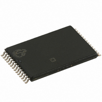
CY62256NLL-70ZRXI Cypress Semiconductor Corp, CY62256NLL-70ZRXI Datasheet - Page 2

CY62256NLL-70ZRXI
Manufacturer Part Number
CY62256NLL-70ZRXI
Description
IC SRAM 256KBIT 70NS 28TSOP
Manufacturer
Cypress Semiconductor Corp
Type
Asynchronousr
Datasheet
1.CY62256NLL-55SNXI.pdf
(13 pages)
Specifications of CY62256NLL-70ZRXI
Memory Size
256K (32K x 8)
Package / Case
28-TSOP I
Format - Memory
RAM
Memory Type
SRAM
Speed
70ns
Interface
Parallel
Voltage - Supply
4.5 V ~ 5.5 V
Operating Temperature
-40°C ~ 85°C
Access Time
70 ns
Supply Voltage (max)
5.5 V
Supply Voltage (min)
4.5 V
Maximum Operating Current
50 mA
Maximum Operating Temperature
+ 85 C
Minimum Operating Temperature
- 40 C
Mounting Style
SMD/SMT
Number Of Ports
1
Operating Supply Voltage
5 V
Lead Free Status / RoHS Status
Lead free / RoHS Compliant
Lead Free Status / RoHS Status
Lead free / RoHS Compliant, Lead free / RoHS Compliant
Available stocks
Company
Part Number
Manufacturer
Quantity
Price
Company:
Part Number:
CY62256NLL-70ZRXI
Manufacturer:
CYPRESS
Quantity:
5 120
Document #: 001-06511 Rev. *A
Product Portfolio
Pin Configurations
Pin Definitions
CY62256NL
CY62256NLL
CY62256NLL
CY62256NLL
CY62256NLL
1–10, 21, 23–26
11–13, 15–19,
27
20
22
14
28
Note:
2. Typical specifications are the mean values measured over a large sample size across normal production process variations and are taken at nominal conditions
(T
A
= 25°C, V
Pin Number
GND
I/O 0
I/O 1
I/O 2
A 10
A 11
A 12
A 13
A 14
A 5
A 6
A 7
A 8
A 9
Product
CC
13
14
1
2
3
4
5
6
7
8
9
10
11
12
Top View
). Parameters are guaranteed by design and characterization, and not 100% tested.
Com’l / Ind’l
Commercial
Industrial
Automotive-A
Automotive-E
DIP
28
27
26
25
24
23
22
21
20
19
18
17
16
15
I/O 3
V CC
WE
A 4
A 3
A 2
A 1
OE
A 0
CE
I/O 7
I/O 6
I/O 5
I/O 4
Input
Input/Output
Input/Control
Input/Control
Input/Control
Ground
Power Supply V
Type
Min.
4.5
A
I/O
WE. When selected LOW, a WRITE is conducted. When selected HIGH, a READ is
conducted
CE. When LOW, selects the chip. When HIGH, deselects the chip
OE. Output Enable. Controls the direction of the I/O pins. When LOW, the I/O pins
behave as outputs. When deasserted HIGH, I/O pins are tri-stated, and act as input
data pins
GND. Ground for the device
CC
0
–A
0
–I/O
. Power supply for the device
V
GND
I/O 0
I/O 1
I/O 2
14
CC
A 10
A 11
A 12
A 13
A 14
A 5
A 6
A 7
A 8
A 9
Typ.
. Address Inputs
7
Range (V)
5.0
. Data lines. Used as input or output lines depending on operation
Narrow SOIC
13
1
2
3
4
5
6
7
8
9
10
11
12
14
[2]
Top View
28
27
26
25
24
23
22
21
20
19
18
17
16
15
Max.
I/O 3
V CC
WE
A 4
A 3
A 2
A 1
OE
A 0
CE
I/O 7
I/O 6
I/O 5
I/O 4
5.5
Speed
Description
55/70
55/70
(ns)
70
70
55
V
V
WE
A
A
A
A
WE
OE
OE
CC
A
A
A
A
A
A
A
A
A
CC
A
A
A
A
A
A
A
A
A
10
11
11
10
1
2
3
4
5
6
8
9
7
9
8
7
6
5
4
3
2
1
22
23
24
25
26
27
28
1
2
3
4
5
6
7
26
25
24
23
22
7
6
5
4
3
2
1
28
27
Typ.
Operating, I
25
25
25
25
25
Reverse Pinout
[2]
(not to scale)
(not to scale)
(mA)
Top View
Top View
TSOP I
Power Dissipation
TSOP I
Max.
50
50
50
50
50
CC
CY62256N
Typ.
Standby, I
0.1
0.1
0.1
0.1
2
10
11
12
13
14
15
16
17
18
19
20
21
21
20
19
18
17
16
15
14
13
12
11
10
8
9
Page 2 of 13
9
8
[2]
(µA)
A
CE
I/O
I/O
I/O
I/O
I/O
GND
I/O
I/O
I/O
A
A
A
A
A
A
I/O
I/O
I/O
GND
I/O
I/O
I/O
I/O
I/O
CE
A
0
14
13
12
12
13
14
0
7
6
5
4
3
2
1
0
0
1
2
3
4
5
6
7
Max.
SB2
50
10
10
15
5
[+] Feedback


