CY62256NLL-70PXC Cypress Semiconductor Corp, CY62256NLL-70PXC Datasheet
CY62256NLL-70PXC
Specifications of CY62256NLL-70PXC
CY62256NLL-70PXC
Available stocks


Related parts for CY62256NLL-70PXC


CY62256NLL-70PXC Summary of contents
Page 1
... Note 1. For best practice recommendations, do refer to the Cypress application note “System Design Guidelines” on http://www.cypress.com Cypress Semiconductor Corporation Document #: 001-06511 Rev. *B 256K (32K x 8) Static RAM Functional Description The CY62256N organized as 32K words by 8 bits. Easy memory expansion is provided by an active LOW chip enable (CE) and active LOW output enable (OE) and tristate drivers ...
Page 2
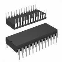
... Product Portfolio Product Min CY62256NL Commercial / 4.5 Industrial CY62256NLL Commercial CY62256NLL Industrial CY62256NLL Automotive-A CY62256NLL Automotive-E Pin Configurations Figure 1. 28-Pin DIP and Narrow SOIC Table 1. Pin Definitions Pin Number Type 1–10, 21, 23–26 Input 11–13, 15–19, Input/Output 27 Input/Control 20 Input/Control 22 Input/Control 14 Ground ...
Page 3
Maximum Ratings Exceeding maximum ratings may impair the useful life of the device. These user guidelines are not tested. Storage Temperature ................................. –65°C to +150°C Ambient Temperature with Power Applied ............................................. -55°C to +125°C Supply Voltage to Ground Potential (Pin ...
Page 4
Thermal Resistance [5] Parameter Description Θ Thermal Resistance JA (Junction to Ambient) Θ Thermal Resistance JC (Junction to Case) R1 1800Ω OUTPUT OUTPUT R2 100 pF 990Ω INCLUDING INCLUDING JIG AND SCOPE (a) Data Retention Characteristics Parameter Description ...
Page 5
... L 10. The internal Write time of the memory is defined by the overlap of CE LOW and WE LOW. Both signals must be LOW to initiate a Write and either signal can terminate a Write by going HIGH. The data input setup and hold timing should be referenced to the rising edge of the signal that terminates the Write. ...
Page 6
Switching Waveforms (continued ACE OE t LZOE HIGH IMPEDANCE DATA OUT t LZCE SUPPLY CURRENT Figure 7. Write Cycle No. 1 (WE Controlled) ADDRESS DATA I/O NOTE t ...
Page 7
Switching Waveforms (continued) Figure 9. Write Cycle No. 3 (WE Controlled, OE LOW) ADDRESS DATA I/O NOTE 17 t HZWE Document #: 001-06511 Rev. *B [11, 16 DATA VALID IN ...
Page 8
Typical DC and AC Characteristics NORMALIZED SUPPLY CURRENT vs. SUPPLY VOLTAGE 1.4 1 1.0 0 25°C A 0.4 0 0.0 4.0 4.5 5.0 5.5 6.0 SUPPLY VOLTAGE (V) NORMALIZED ...
Page 9
Typical DC and AC Characteristics TYPICAL POWER-ON CURRENT vs. SUPPLY VOLTAGE 3.0 2.5 2.0 1.5 1.0 0.5 0.0 0.0 1.0 2.0 3.0 4.0 5.0 SUPPLY VOLTAGE (V) Truth Table Inputs/Outputs High ...
Page 10
... CY62256NL−70SNXC CY62256NLL−70SNC CY62256NLL−70SNXC CY62256NLL−70ZC CY62256NLL−70ZXC CY62256NL–70SNI CY62256NL–70SNXI CY62256NLL−70SNI CY62256NLL−70SNXI CY62256NLL−70ZI CY62256NLL−70ZXI CY62256NLL−70ZRI CY62256NLL−70ZRXI CY62256NLL−70SNXA Do contact your local Cypress sales representative for availability of these parts Document #: 001-06511 Rev. *B ...
Page 11
Package Diagrams Figure 10. 28-Pin (600-Mil) Molded DIP (51-85017) Figure 11. 28-Pin (300-mil) SNC (Narrow Body) (51-85092) Document #: 001-06511 Rev. *B CY62256N 51-85017-*C 51-85092-*B Page [+] Feedback ...
Page 12
Figure 12. 28-Pin TSOP 13.4 mm) (51-85071) Document #: 001-06511 Rev. *B CY62256N 51-85071-*G Page [+] Feedback ...
Page 13
Figure 13. 28-Pin TSOP 13.4 mm) (51-85074) Document #: 001-06511 Rev. *B CY62256N 51-85074-*F Page [+] Feedback ...
Page 14
... Cypress against all charges. Any Source Code (software and/or firmware) is owned by Cypress Semiconductor Corporation (Cypress) and is protected by and subject to worldwide patent protection (United States and foreign), United States copyright laws and international treaty provisions. Cypress hereby grants to licensee a personal, non-exclusive, non-transferable license to copy, use, modify, create derivative works of, and compile the Cypress Source Code and derivative works for the sole purpose of creating custom software and or firmware in support of licensee product to be used only in conjunction with a Cypress integrated circuit as specified in the applicable agreement ...