CY62126EV30LL-45ZSXI Cypress Semiconductor Corp, CY62126EV30LL-45ZSXI Datasheet
CY62126EV30LL-45ZSXI
Specifications of CY62126EV30LL-45ZSXI
CY62126EV30LL-45ZSXI
Available stocks


Related parts for CY62126EV30LL-45ZSXI

CY62126EV30LL-45ZSXI Summary of contents
Page 1
... Cypress Semiconductor Corporation Document #: 38-05486 Rev. *H 1-Mbit (64K x 16) Static RAM advanced circuit design to provide ultra low active current. This is ideal for providing More Battery Life(MoBL applications such as cellular telephones. The device also has an automatic power down feature that significantly reduces power consumption when addresses are not toggling ...
Page 2
Contents Pin Configuration ............................................................. 3 Maximum Ratings............................................................. 4 Operating Range............................................................... 4 Electrical Characteristics................................................. 4 Capacitance ...................................................................... 5 Thermal Resistance.......................................................... 5 Data Retention Characteristics ....................................... 6 Switching Characteristics................................................ 7 Switching Waveforms ...................................................... 8 Truth Table ...................................................................... 11 Document #: 38-05486 Rev. ...
Page 3
... Table 1. Product Portfolio Product Range Min CY62126EV30LL Industrial 2.2 CY62126EV30LL Automotive 2.2 Notes 1. NC pins are not connected on the die. 2. Typical values are included for reference only and are not guaranteed or tested. Typical values are measured at V Document #: 38-05486 Rev ...
Page 4
... Chip enable (CE) needs to be tied to CMOS levels to meet the I Document #: 38-05486 Rev input voltage Output current into outputs (LOW) .............................. 20 mA Static discharge voltage.......................................... > 2001 V (MIL-STD-883, Method 3015) Latch up current..................................................... > 200 mA Operating Range + 0.3 V) CCmax Device CY62126EV30LL + 0.3 V) CCmax 45 ns (Industrial) Test Conditions Min = –0.1 mA 2.0 = –1.0 mA, V > 2.70V 2 ...
Page 5
Capacitance For all packages. Tested initially and after any design or process changes that may affect these parameters. Parameter Description C Input capacitance IN C Output capacitance OUT Thermal Resistance Tested initially and after any design or process changes that ...
Page 6
Data Retention Characteristics Over the Operating Range Parameter Description V V for data retention DR CC [9] I Data retention current CCDR [10] t Chip deselect to data CDR retention time [10] t Operation recovery time ...
Page 7
... HZOE HZCE HZBE HZWE 15. The internal write time of the memory is defined by the overlap of WE signals can terminate a write by going inactive. The data input setup and hold timing must refer to the edge of signal that terminates write. Document #: 38-05486 Rev (Industrial) Min ...
Page 8
Switching Waveforms Figure 5. Read Cycle No. 1(Address transition controlled) ADDRESS DATA OUT PREVIOUS DATA VALID Figure 6. Read Cycle No. 2 (OE controlled) ADDRESS CE t ACE OE t LZOE BHE/BLE t LZBE HIGH IMPEDANCE DATA OUT t LZCE ...
Page 9
... DATA I/O NOTE 22 t HZOE Notes 19. The internal write time of the memory is defined by the overlap of WE these signals can terminate a write by going inactive. The data input setup and hold timing must refer to the edge of signal that terminates write. 20. Data I/O is high impedance ...
Page 10
Switching Waveforms (continued) Figure 9. Write Cycle No. 3 (WE controlled, OE LOW ADDRESS CE BHE/BLE DATA I/O NOTE 24 Figure 10. Write Cycle No. 4 (BHE/BLE controlled, OE LOW) ADDRESS CE BHE/BLE NOTE ...
Page 11
Truth Table [25 BHE ...
Page 12
... Ordering Information Speed (ns) Ordering Code 45 CY62126EV30LL-45BVXI CY62126EV30LL-45ZSXI CY62126EV30LL-45ZSXA 55 CY62126EV30LL-55BVXE CY62126EV30LL-55ZSXE Contact your local Cypress sales representative for availability of other parts. Ordering Code Definitions 45/55 CY 621 V30 LL Document #: 38-05486 Rev. *H Package Package Type Diagram 51-85150 48-ball VFBGA (Pb-free) 51-85087 44-pin TSOP II (Pb-free) ...
Page 13
Package Diagrams Document #: 38-05486 Rev. *H Figure 11. 48-Ball VFBGA ( mm), 51-85150 CY62126EV30 MoBL 51-85150 *F Page ...
Page 14
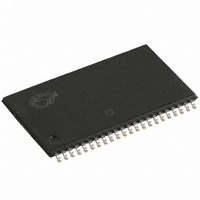
... CMOS complementary metal oxide semiconductor CE chip enable I/O input/output OE output enable SRAM static random access memory TSOP thin small outline package VFBGA very fine ball gird array WE write enable Document #: 38-05486 Rev. *H Figure 12. 44-Pin TSOP II, 51-85087 PIN 1 I.D. ...
Page 15
... Removed byte enable from footnote #2 in Added footnote related to chip enable in Updated Package Diagrams Updated links in Sales, Solutions, and Legal Information AJU Added CY62126EV30LL-45ZSXA part in Added Ordering Code Definitions. Modified table footnote format. PRAS Updated Figure 1 and Package Diagram, and fixed Typo in Figure 3.. ...
Page 16
... Cypress against all charges. Any Source Code (software and/or firmware) is owned by Cypress Semiconductor Corporation (Cypress) and is protected by and subject to worldwide patent protection (United States and foreign), United States copyright laws and international treaty provisions. Cypress hereby grants to licensee a personal, non-exclusive, non-transferable license to copy, use, modify, create derivative works of, and compile the Cypress Source Code and derivative works for the sole purpose of creating custom software and or firmware in support of licensee product to be used only in conjunction with a Cypress integrated circuit as specified in the applicable agreement ...