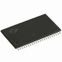
CY7C1021BNV33L-15ZXI Cypress Semiconductor Corp, CY7C1021BNV33L-15ZXI Datasheet

CY7C1021BNV33L-15ZXI
Specifications of CY7C1021BNV33L-15ZXI
Available stocks
Related parts for CY7C1021BNV33L-15ZXI
CY7C1021BNV33L-15ZXI Summary of contents
Page 1
... Available in a 48-ball Mini BGA package ■ Note 1. For guidelines on SRAM system design, please refer to the ‘System Design Guidelines’ Cypress application note, available on the internet at www.cypress.com. Cypress Semiconductor Corporation Document #: 001-06433 Rev. *C Functional Description The CY7C1021BNV33 is a high-performance CMOS static RAM organized as 65,536 words by 16 bits ...
Page 2
Logic Block Diagram DATA IN DRIVERS COLUMN DECODER Selection Guide Maximum Access Time (ns) Maximum Operating Current (mA) Maximum CMOS Standby Current (mA) Document ...
Page 3
Contents Pin Configurations ........................................................... 4 Maximum Ratings ............................................................. 5 Operating Range ............................................................... 5 Electrical Characteristics ................................................. 5 Capacitance ...................................................................... 5 AC Test Loads and Waveforms ....................................... 6 Switching Characteristics ................................................ 7 Data Retention Characteristics ....................................... 8 Data Retention Waveform ................................................ ...
Page 4
Pin Configurations Document #: 001-06433 Rev. *C SOJ / TSOP II Top View BHE ...
Page 5
Maximum Ratings Exceeding maximum ratings may shorten the useful life of the device. User guidelines are not tested. Storage Temperature ............................... –65 °C to +150 °C Ambient Temperature with Power Applied .......................................... –55 °C to +125 °C [2] Supply Voltage ...
Page 6
AC Test Loads and Waveforms R 317 3.3 V 3.3 V OUTPUT OUTPUT 351 INCLUDING INCLUDING JIG AND JIG AND SCOPE SCOPE (a) OUTPUT Equivalent to: THÉVENIN EQUIVALENT Document #: 001-06433 Rev 317 3.0 V ...
Page 7
... At any given temperature and voltage condition The internal write time of the memory is defined by the overlap of CE LOW, WE LOW and BHE / BLE LOW. CE, WE and BHE / BLE must be LOW to initiate a write, and the transition of these signals can terminate the write. The input data set-up and hold timing should be referenced to the leading edge of the signal that terminates the write ...
Page 8
Data Retention Characteristics Over the Operating Range (L version only) Parameter Description V V for Data Retention Data Retention Current CCDR [9] t Chip Deselect to Data Retention Time CDR [10] t Operation Recovery Time R Data ...
Page 9
Switching Waveforms [11, 12] Read Cycle No. 1 ADDRESS DATA OUT PREVIOUS DATA VALID Read Cycle No. 2 (OE Controlled) ADDRESS CE t ACE OE t DOE BHE, BLE t LZOE t DBE t LZBE HIGH IMPEDANCE DATA OUT t ...
Page 10
Switching Waveforms (continued) Write Cycle No. 1 (CE Controlled) ADDRESS BHE, BLE DATA I/O Write Cycle No. 2 (BLE or BHE Controlled) ADDRESS t SA BHE, BLE WE CE DATA I/O Notes 14. Data I/O is ...
Page 11
Switching Waveforms (continued) Write Cycle No. 2 (WE Controlled, OE LOW) ADDRESS BHE, BLE DATA I/O Truth Table BLE BHE I High ...
Page 12
... For a complete listing of all options, visit the Cypress website at and refer to the product summary page at Cypress maintains a worldwide network of offices, solution centers, manufacturer’s representatives and distributors. To find the office closest to you, visit us at http://www.cypress.com/go/datasheet/offices. Speed (ns) Ordering Code 15 CY7C1021BNV33L-15BAI CY7C1021BNV33L-15VXI CY7C1021BNV33L-15ZXI Ordering Code Definitions V33 L Please contact local sales representative regarding availability of these parts ...
Page 13
Package Diagrams Figure 1. 48-ball FBGA (7 mm × × 1.2 mm), 51-85096 Figure 2. 44-pin (400-Mil) Molded SOJ, 51-85082 Document #: 001-06433 Rev. *C CY7C1021BNV33 51-85096 *I 51-85082 *C Page [+] Feedback ...
Page 14
Package Diagrams (continued) Document #: 001-06433 Rev. *C Figure 3. 44-pin TSOP Type II, 51-85087 CY7C1021BNV33 51-85087 *C Page [+] Feedback ...
Page 15
... CE chip enable FBGA Fine-Pitch Ball Grid Array I/O input/output OE output enable SOJ small outline J-lead SRAM static random access memory TTL transistor-transistor logic TSOP thin small-outline package WE write enable Document #: 001-06433 Rev. *C CY7C1021BNV33 Document Conventions Units of Measure Symbol ...
Page 16
Document History Page Document Title: CY7C1021BNV33 64 K × 16 Static RAM Document Number: 001-06433 Orig. of REV. ECN NO. Issue Date Change ** 423847 See ECN *A 2897061 03/22/10 *B 3109897 12/14/2010 *C 3103073 03/08/2011 Document #: 001-06433 Rev. ...
Page 17
... Cypress against all charges. Any Source Code (software and/or firmware) is owned by Cypress Semiconductor Corporation (Cypress) and is protected by and subject to worldwide patent protection (United States and foreign), United States copyright laws and international treaty provisions. Cypress hereby grants to licensee a personal, non-exclusive, non-transferable license to copy, use, modify, create derivative works of, and compile the Cypress Source Code and derivative works for the sole purpose of creating custom software and or firmware in support of licensee product to be used only in conjunction with a Cypress integrated circuit as specified in the applicable agreement ...


