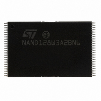
NAND128W3A2BN6E NUMONYX, NAND128W3A2BN6E Datasheet - Page 30

NAND128W3A2BN6E
Manufacturer Part Number
NAND128W3A2BN6E
Description
IC FLASH 128MBIT 48TSOP
Manufacturer
NUMONYX
Specifications of NAND128W3A2BN6E
Format - Memory
FLASH
Memory Type
FLASH - Nand
Memory Size
128M (16M x 8)
Interface
Parallel
Voltage - Supply
2.7 V ~ 3.6 V
Operating Temperature
-40°C ~ 85°C
Package / Case
48-TSOP
Access Time
12µs
Supply Voltage Range
2.7V To 3.6V
Memory Case Style
TSOP
No. Of Pins
48
Operating Temperature Range
-40°C To +85°C
Voltage, Vcc
3.3V
Rohs Compliant
Yes
Lead Free Status / RoHS Status
Lead free / RoHS Compliant
Speed
-
Lead Free Status / RoHS Status
Lead free / RoHS Compliant, Lead free / RoHS Compliant
Other names
497-5037
497-5037
497-5037
Available stocks
Company
Part Number
Manufacturer
Quantity
Price
Company:
Part Number:
NAND128W3A2BN6E
Manufacturer:
MICRON
Quantity:
3 000
Part Number:
NAND128W3A2BN6E
Manufacturer:
ST
Quantity:
20 000
NAND128-A, NAND256-A, NAND512-A, NAND01G-A
Figure 22. Bad Block Management Flowchart
Figure 23. Garbage Collection
Garbage Collection
When a data page needs to be modified, it is faster
to write to the first available page, and the previous
page is marked as invalid. After several updates it
is necessary to remove invalid pages to free some
memory space.
To free this memory space and allow further pro-
gram operations it is recommended to implement
a Garbage Collection algorithm. In a Garbage Col-
lection software the valid pages are copied into a
free area and the block containing the invalid pag-
es is erased (see
30/56
Block Address =
START
Block 0
= FFh?
block?
Data
Last
END
YES
YES
Figure
Invalid
Valid
Page
Page
NO
NO
23.).
Bad Block table
Update
Block Address
Increment
Old Area
AI07588C
(Erased)
Free
Page
Wear-leveling Algorithm
For write-intensive applications, it is recommend-
ed to implement a Wear-leveling Algorithm to
monitor and spread the number of write cycles per
block.
In memories that do not use a Wear-Leveling Al-
gorithm not all blocks get used at the same rate.
Blocks with long-lived data do not endure as many
write cycles as the blocks with frequently-changed
data.
The Wear-leveling Algorithm ensures that equal
use is made of all the available write cycles for
each block. There are two wear-leveling levels:
New Area (After GC)
AI07599B


