CY7C136-25JXC Cypress Semiconductor Corp, CY7C136-25JXC Datasheet
CY7C136-25JXC
Specifications of CY7C136-25JXC
CY7C136-25JXC
Available stocks


Related parts for CY7C136-25JXC


CY7C136-25JXC Summary of contents
Page 1
... INT L Notes 1. CY7C136 and CY7C136A are functionally identical. 2. CY7C132/CY7C136/CY7C136A (Master): BUSY is open drain output and requires pull up resistor. CY7C142/CY7C146 (Slave): BUSY is input. 3. Open drain outputs; pull up resistor required. Cypress Semiconductor Corporation Document #: 38-06031 Rev. *G CY7C136A, CY7C142, CY7C146 Dual-Port Static RAM ...
Page 2
... Selection Guide Specification Maximum Access Time Maximum Operating Current Com’l/Ind Maximum Standby Current Com’l/Ind Shaded areas contain preliminary information. Note and 25 ns version available in PQFP and PLCC packages only. Document #: 38-06031 Rev. *G CY7C136A, CY7C142, CY7C146 Figure 2. 52-Pin PQFP (Top View ...
Page 3
... Duration of the short circuit should not exceed 30 seconds address and data inputs are cycling at the maximum frequency of read cycle of 1/t MAX Document #: 38-06031 Rev. *G CY7C136A, CY7C142, CY7C146 DC Input Voltage ................................................. −3.5V to +7.0V Output Current into Outputs (LOW)............................. 20 mA Static Discharge Voltage.......................................... > 2001V (per MIL-STD-883, Method 3015) Latch up Current.................................................... > ...
Page 4
... At any given temperature and voltage condition for any given device and t are tested with C LZCE LZWE HZOE LZOE, HZCE, HZWE voltage. Document #: 38-06031 Rev. *G CY7C136A, CY7C142, CY7C146 Test Conditions T = 25° MHz 5. Figure 3. AC Test Loads and Waveforms R1 893Ω 5V OUTPUT 347Ω INCLUDING JIG AND ...
Page 5
... A write operation on Port A, where Port A has priority, leaves the data on Port B’s outputs undisturbed until one access time after one of the following: BUSY on Port B goes HIGH. Port B’s address toggled. CE for Port B is toggled. R/W for Port B is toggled during valid read. 16. 52-pin PLCC and PQFP versions only. Document #: 38-06031 Rev. *G CY7C136A, CY7C142, CY7C146 [8] (continued) 7C132-25 [4] 7C136-15 7C146-15 ...
Page 6
... R/W LOW after BUSY LOW WB t R/W HIGH after BUSY HIGH WH t BUSY HIGH to Valid Data BDD t Write Data Valid to Read Data Valid DDD t Write Pulse to Data Delay WDD Document #: 38-06031 Rev. *G CY7C136A, CY7C142, CY7C146 [8] 7C132-35 7C136-35 7C142-35 7C146-35 Min Max ...
Page 7
... Figure 5. Read Cycle No. 2 (Either Port-CE/ LZOE t LZCE DATA OUT Notes 17. R/W is HIGH for read cycle. 18. Device is continuously selected and 19. Address valid prior to or coincident with CE transition LOW. Document #: 38-06031 Rev. *G CY7C136A, CY7C142, CY7C146 [8] (continued) 7C132-35 7C136-35 7C142-35 7C146-35 Min Max [13] 25 [13] 25 [13 ...
Page 8
... Switching Waveforms (continued) Figure 6. Read Cycle No. 3 (Read with BUSY Master: CY7C132 and CY7C136/CY7C136A) ADDRESS R R INR t PS ADDRESS L BUSY L DOUT L Figure 7. Write Cycle No.1 (OE Three-States Data I/Os—Either Port) ADDRESS R/W DATA HZOE D OUT Note 20 LOW during a R/W controlled write cycle, the write pulse width must be the larger of t and for data to be placed on the bus for the required t Document #: 38-06031 Rev ...
Page 9
... R CE Valid First: R ADDRESS L BUSY L Note 21. If the CE LOW transition occurs simultaneously with or after the R/W LOW transition, the outputs remain in a high impedance state. Document #: 38-06031 Rev. *G CY7C136A, CY7C142, CY7C146 SCE PWE t SD DATA VALID t HZWE HIGH IMPEDANCE ADDRESS MATCH ...
Page 10
... PS ADDRESS R BUSY R Right Address Valid First: ADDRESS ADDRESS MATCH ADDRESS L BUSY L Figure 11. Busy Timing Diagram No. 3 (Write with BUSY, Slave: CY7C142/CY7C146 BUSY Document #: 38-06031 Rev. *G CY7C136A, CY7C142, CY7C146 ADDRESS MISMATCH t t BLA BHA ADDRESS MISMATCH t t BLA BHA t PWE t WH ...
Page 11
... INT R ADDRESS R INT L ADDRESS INT L Document #: 38-06031 Rev. *G CY7C136A, CY7C142, CY7C146 Figure 12. Left Side Sets INT WRITE 7FF t t INS HA t EINS t WINS Figure 13. Right Side Clears INT EINR Figure 14. Right Side Sets INT t WC WRITE 7FE t t INS HA t EINS ...
Page 12
... SUPPLY VOLTAGE (V) TYPICAL POWER-ON CURRENT vs. SUPPLY VOLTAGE 3.0 2.5 2.0 1.5 1.0 0.5 0.0 0 1.0 2.0 3.0 4.0 SUPPLY VOLTAGE (V) Document #: 38-06031 Rev. *G CY7C136A, CY7C142, CY7C146 Figure 16. Typical DC and AC Characteristics NORMALIZED SUPPLY CURRENT vs. AMBIENT TEMPERATURE 1 1.0 0 5.0V IN 0.4 0.2 ...
Page 13
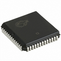
... Ordering Information Speed Ordering Code (ns) 25 CY7C136-25JXC CY7C136-25NC CY7C136-25NXC CY7C136-25JXI 55 CY7C136-55JC CY7C136-55JXC CY7C136-55NC CY7C136-55NXC CY7C136A-55JXI CY7C136A-55NXI 55 CY7C146-55JXC Ordering Code Definitions XXX Document #: 38-06031 Rev. *G CY7C136A, CY7C142, CY7C146 Package Package Type Diagram 51-85004 52-Pin Plastic Leaded Chip Carrier (Pb-Free) 51-85042 52-Pin Plastic Quad Flatpack ...
Page 14
... Package Diagrams Figure 17. 52-Pin Plastic Leaded Chip Carrier, 51-85004 Figure 18. 52-Pin Plastic Quad Flatpack, 51-85042 Document #: 38-06031 Rev. *G CY7C132, CY7C136 CY7C136A, CY7C142, CY7C146 51-85004 *B 51-85042 *A Page [+] Feedback ...
Page 15
... Removed cross information from features section YIM Added Pb-Free Logo Added Pb-Free parts to ordering information: CY7C136-25JXC, CY7C136-25NXC, CY7C136-55JXC, CY7C136-55NXC, CY7C136-55JXI, CY7C136-55NXI, CY7C146-25JXC, CY7C146-55JXC Removed CY7C132/142 from the Ordering information table Removed 48-Pin DIP and 52-Pin Square LCC package from the data sheet ...