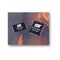
SST49LF080A-33-4C-NHE Microchip Technology, SST49LF080A-33-4C-NHE Datasheet - Page 22

SST49LF080A-33-4C-NHE
Manufacturer Part Number
SST49LF080A-33-4C-NHE
Description
IC FLASH SER LPC 8MBIT 32PLCC
Manufacturer
Microchip Technology
Datasheets
1.SST49LF080A-33-4C-NHE.pdf
(49 pages)
2.SST49LF080A-33-4C-NHE.pdf
(2 pages)
3.SST49LF080A-33-4C-NHE.pdf
(2 pages)
Specifications of SST49LF080A-33-4C-NHE
Memory Type
FLASH
Memory Size
8M (1M x 8)
Operating Temperature
0°C ~ 85°C
Package / Case
32-PLCC
Format - Memory
FLASH
Speed
33MHz
Interface
Parallel
Voltage - Supply
3 V ~ 3.6 V
Data Bus Width
8 bit
Architecture
Sectored
Interface Type
LPC
Access Time
33 ns
Supply Voltage (max)
3.6 V
Supply Voltage (min)
3 V
Maximum Operating Current
12 mA
Mounting Style
SMD/SMT
Organization
1024 KB x 8
Lead Free Status / RoHS Status
Lead free / RoHS Compliant
Lead Free Status / RoHS Status
Lead free / RoHS Compliant, Lead free / RoHS Compliant
Available stocks
Company
Part Number
Manufacturer
Quantity
Price
Company:
Part Number:
SST49LF080A-33-4C-NHE
Manufacturer:
Microchip Technology
Quantity:
10 000
Part Number:
SST49LF080A-33-4C-NHE
Manufacturer:
SST
Quantity:
20 000
Company:
Part Number:
SST49LF080A-33-4C-NHE-T
Manufacturer:
Microchip Technology
Quantity:
10 000
Part Number:
SST49LF080A-33-4C-NHE-T
Manufacturer:
SST
Quantity:
20 000
Data Sheet
©2006 Silicon Storage Technology, Inc.
LFRAME#
LFRAME#
LFRAME#
LAD[3:0]
LAD[3:0]
LAD[3:0]
FIGURE 8: Data# Polling Command Sequence (LPC Mode)
LCLK
LCLK
LCLK
CE#
CE#
CE#
Note: 1. Address must be within memory address range specified in Table 4.
Start
Start
1 Clock 1 Clock
1 Clock 1 Clock
0000b
0000b
1st Start
1 Clock 1 Clock
0000b 011Xb
Memory
Memory
010Xb
010Xb
Read
Cycle
Read
Cycle
Memory
Cycle
Write
A[31:28] A[27:24]
A[31:28] A[27:24]
A[31:28] A[27:24]
A[23:20] A[19:16]
A[23:20] A[19:16]
Load Address in 8 Clocks
Load Address in 8 Clocks
A[23:20] A[19:16]
Write the last command (Program or Erase) to the device in LPC mode.
When internal write complete, the DQ 7 will equal to D7.
Load Address in 8 Clocks
Read the DQ 7 to see if internal write complete or not.
Address 1
Address 1
Address 1
A[15:12]
A[15:12]
A[15:12]
A[11:8]
A[11:8]
22
A[11:8]
A[7:4]
A[7:4]
A[7:4]
A[3:0]
A[3:0]
A[3:0]
1111b
1111b
Load Data in 2 Clocks
2 Clocks
2 Clocks
D[3:0]
TAR
TAR
Tri-State
Tri-State
Data
Dn[7:4]
1 Clock
1 Clock
0000b
0000b
Sync
Sync
1111b
2 Clocks
Data out 2 Clocks
Data out 2 Clocks
XXXXb
XXXXb
TAR
Tri-State
Data
Data
8 Mbit LPC Flash
D7,xxx
D7#,xxx
1 Clock
0000b
Sync
SST49LF080A
S71235-02-000
TAR
TAR
TAR
1235 F07.0
Next start
Next start
1 Clock
1 Clock
0000b
0000b
Command
Start next
1 Clock
0000b
5/06


