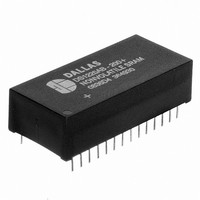
DS1225AD-200+ Maxim Integrated Products, DS1225AD-200+ Datasheet - Page 7

DS1225AD-200+
Manufacturer Part Number
DS1225AD-200+
Description
IC NVSRAM 64KBIT 200NS 28DIP
Manufacturer
Maxim Integrated Products
Datasheet
1.DS1225AD-150.pdf
(9 pages)
Specifications of DS1225AD-200+
Format - Memory
RAM
Memory Type
NVSRAM (Non-Volatile SRAM)
Memory Size
64K (8K x 8)
Speed
200ns
Interface
Parallel
Voltage - Supply
4.5 V ~ 5.5 V
Operating Temperature
0°C ~ 70°C
Package / Case
28-DIP Module (600 mil), 28-EDIP
Data Bus Width
8 bit
Organization
8 K x 8
Interface Type
Parallel
Access Time
200 ns
Supply Voltage (max)
5.5 V
Supply Voltage (min)
4.5 V
Operating Current
75 mA
Maximum Operating Temperature
+ 70 C
Minimum Operating Temperature
0 C
Mounting Style
Through Hole
Lead Free Status / RoHS Status
Lead free / RoHS Compliant
NOTES:
1. WE is high for a read cycle.
2. OE = V
3. t
4. t
5. These parameters are sampled with a 5 pF load and are not 100% tested.
6. If the CE low transition occurs simultaneously with or later than the WE low transition, the output
7. If the CE high transition occurs prior to or simultaneously with the WE high transition, the output
8. If WE is low or the WE low transition occurs prior to or simultaneously with the CE low transition,
9. Each DS1225AB and each DS1225AD has a built-in switch that disconnects the lithium source until
10. All AC and DC electrical characteristics are valid over the full operating temperature range. For
11. In a power down condition the voltage on any pin may not exceed the voltage on V
12. t
13. t
14. DS1225 modules are recognized by Underwriters Laboratories (UL) under file E99151.
DC TEST CONDITIONS
Outputs Open
Cycle = 200ns for Operating Current
All Voltages Are Referenced to Ground
state.
going low to the earlier of CE or WE going high.
buffers remain in a high-impedance state during this period.
buffers remain in a high-impedance state during this period.
the output buffers remain in a high-impedance state during this period.
V
V
and is not 100% tested.
commercial products, this range is 0°C to 70°C. For industrial products (IND), this range is -40°C to
+85°C.
WP
DS
WR1
WR2
CC
CC
are measured from the earlier of CE or WE going high.
is specified as the logical AND of CE and WE . t
starting from the time power is first applied by the user. This parameter is guaranteed by design
is first applied by the user. The expected t
, t
, t
DH1
DH2
IH
are measured from WE going high.
are measured from CE going high.
or V
IL
. If OE = V
IH
during write cycle, the output buffers remain in a high-impedance
7 of 9
DR
is defined as accumulative time in the absence of
AC TEST CONDITIONS
Output Load: 100 pF + 1TTL Gate
Input Pulse Levels: 0 - 3.0V
Timing Measurement Reference Levels
Input Pulse Rise and Fall Times: 5ns
WP
is measured from the latter of CE or WE
Input: 1.5V
Output: 1.5V
CC
.
DS1225AB/AD


