CY7C1024DV33-10BGXI Cypress Semiconductor Corp, CY7C1024DV33-10BGXI Datasheet
CY7C1024DV33-10BGXI
Specifications of CY7C1024DV33-10BGXI
Available stocks


Related parts for CY7C1024DV33-10BGXI

CY7C1024DV33-10BGXI Summary of contents
Page 1
... Cypress Semiconductor Corporation Document Number: 001-08353 Rev. *C 3-Mbit (128K X 24) Static RAM Functional Description The CY7C1024DV33 is a high performance CMOS static RAM organized as 128K words by 24 bits. This device has an automatic power down feature that significantly reduces power consumption when deselected. ...
Page 2
... Maximum CMOS Standby Current Pin Configuration Note 1. NC pins are not connected on the die. Document Number: 001-08353 Rev. *C [1] Figure 1. 119-Ball PBGA Top View CY7C1024DV33 –10 Unit 10 ns 175 Page [+] Feedback [+] Feedback ...
Page 3
... MHz 3. Test Conditions Still air, soldered × 4.5 inch, four layer printed circuit board . CE is LOW when are LOW and CE is HIGH HIGH when CY7C1024DV33 [2] ............................... –0. 0.5V CC Ambient V CC Temperature 3.3V ± 0.3V –40°C to +85°C –10 Unit Min Max 2 ...
Page 4
... GND (c) Description [3] [3, 7] [3, 7] [ the data retention (V , 2.0V) voltage. DD CCDR values until the first memory access is performed. CC CY7C1024DV33 [4] R1 317 Ω 3.3V OUTPUT R2 5 pF* 351Ω * Including jig and scope (b) 10% Fall Time:> 1V/ns –10 Unit Min Max μs ...
Page 5
... CE > V – 0.2V > V – 0. < 0. DATA RETENTION MODE 3.0V > CDR and CE and CE LOW and WE LOW. Chip enables must be active and WE must be LOW and t HZWE > 50 μs or stable at V > 50 μ CC(min) CC(min) CY7C1024DV33 –10 Unit Min Max 5 Min Typ Max ...
Page 6
... If CE goes HIGH simultaneously with WE going HIGH, the output remains in a high impedance state. Document Number: 001-08353 Rev OHA DOE DATA VALID 50 SCE SCE PWE t SD DATA VALID CY7C1024DV33 [13, 14] DATA VALID [3, 14, 15] t HZOE t HZCE HIGH IMPEDANCE t PD ICC 50% ISB [3, 16, 17 Page [+] Feedback [+] Feedback ...
Page 7
... SCE PWE t SD DATA VALID I/O – I/O Mode 0 23 High Z Power Down High Z Power Down High Z Power Down Full Data Out Read Full Data In Write High Z Selected, Outputs Disabled Active (I CY7C1024DV33 [3, 16, 17 [3, 17 LZWE Power Standby ( Standby ( Standby ( Active ( Active (I ...
Page 8
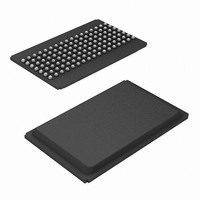
... Ordering Information Speed Ordering Code (ns) 10 CY7C1024DV33-10BGXI Package Diagram Document Number: 001-08353 Rev. *C Package Package Type Name 51-85115 119-Ball Plastic Ball Grid Array ( 2.4 mm) (Pb-Free) Figure 8. 119-Ball PBGA ( 2.4 mm) CY7C1024DV33 Operating Range Industrial 51-85115-*B Page [+] Feedback [+] Feedback ...
Page 9
... Document History Page Document Title: CY7C1024DV33, 3-Mbit (128K X 24) Static RAM Document Number: 001-08353 Orig. of Submission Rev. ECN No. Change Date ** 469517 NXR See ECN *A 499604 NXR See ECN *B 1462586 VKN/SFV See ECN *C 2604677 VKN/PYRS 11/12/08 Sales, Solutions, and Legal Information Worldwide Sales and Design Support Cypress maintains a worldwide network of offices, solution centers, manufacturer’ ...