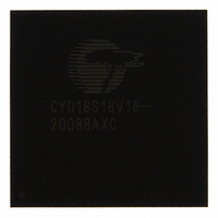
CYD18S18V18-200BBAXC Cypress Semiconductor Corp, CYD18S18V18-200BBAXC Datasheet - Page 15

CYD18S18V18-200BBAXC
Manufacturer Part Number
CYD18S18V18-200BBAXC
Description
IC SRAM 18MBIT 200MHZ 256LFBGA
Manufacturer
Cypress Semiconductor Corp
Datasheet
1.CYD02S36V18-167BBC.pdf
(52 pages)
Specifications of CYD18S18V18-200BBAXC
Memory Size
18M (1M x 18)
Format - Memory
RAM
Memory Type
SRAM - Dual Port, Synchronous
Speed
200MHz
Interface
Parallel
Voltage - Supply
1.42 V ~ 1.58 V, 1.7 V ~ 1.9 V
Operating Temperature
0°C ~ 70°C
Package / Case
256-LFBGA
Memory Configuration
1M X 18
Clock Frequency
77MHz
Access Time
3.3ns
Supply Voltage Range
1.42V To 1.58V, 1.7V To 1.9V
Memory Case Style
BGA
No. Of Pins
256
Rohs Compliant
Yes
Lead Free Status / RoHS Status
Lead free / RoHS Compliant
Other names
428-2036
Available stocks
Company
Part Number
Manufacturer
Quantity
Price
Company:
Part Number:
CYD18S18V18-200BBAXC
Manufacturer:
Cypress Semiconductor Corp
Quantity:
10 000
Increment Operation
After the address counter is initially loaded with an external
address, the counter can internally increment the address value
and address the entire memory array. Only the unmasked bits of
the counter register are incremented. For a counter bit to
change, the corresponding bit in the mask register must be 1. If
the two least significant bits of the mask register are 11, the burst
counter increments by one. If the two least significant bits are 10,
the burst counter increments by two, and if they are 00, the burst
counter increments by four. If all unmasked counter bits are
incremented to 1 and WRP is deasserted, the next increment l
wraps the counter back to the initially loaded value. The cycle
before the increment that results in all unmasked counter bits to
become 1s, a counter interrupt flag (CNTINT) is asserted if the
counter is incremented again. This increment causes the counter
to reach its maximum value and the next increment returns the
counter register to its initial value that was stored in the mirror
register if WRP is deasserted. If WRP is asserted, the unmasked
portion of the counter is filled with 0 instead. The example shown
in
CYDD36S18V18 device with the mask register loaded with a
mask value of 00007F unmasking the seven least significant bits.
Setting the mask register to this value enables the counter to
access the entire memory space. The address counter is then
loaded with an initial value of 000005 assuming WRP is
deasserted. The masked bits, the seventh address through the
twenty-first address, do not increment in an increment operation.
The counter address starts at address 000005 and increments
its internal address value until it reaches the mask register value
of 00007F. The counter wraps around the memory block to
location 000005 at the next count. CNTINT is issued when the
counter reaches the maximum –1 count.
Hold Operation
The value of all three registers is constantly maintained
unchanged for an unlimited number of clock cycles. This
operation is useful in applications where wait states are needed
or when address is available a few cycles ahead of data in a
shared bus interface.
Retransmit
Retransmit enables repeated access to the same block of
memory without the need to reload the initial address. An internal
Note
Document Number: 38-06082 Rev. *J
30. The CYD36S18V18 device has 21 address bits. The CYD36S36V18 and CYD18S18V18 devices have 20 address bits. The CYD36S72V18, CYD18S36V18, and
CYD09S18V18 devices have 19 address bits. The CYD18S72V18, CYD09S36V18, and CYD04S18V18 devices have 18 address bits. The CYD09S72V18 and
CYD04S36V18 devices have 17 address bits. The CYD04S72V18 and CYD02S36V18 have 16 address bits.
Figure 8
on
page 17
[30]
shows
an
example
of
the
mirror register stores the address counter value last loaded.
While RET is asserted low, the counter continues to wrap back
to the value in the mirror register independent of the state of
WRP.
Counter Interrupt
The counter interrupt (CNTINT) is asserted LOW one clock cycle
before an increment operation that results in the unmasked
portion of the counter register being all 1s. It is deasserted by
counter reset, counter load, counter increment, mask reset,
mask load, and MRST.
Counting by Two
When the two least significant bits of the mask register are 10,
the counter increments by two.
Counting by Four
When the two least significant bits of the mask register are 00,
the counter increments by four.
Mailbox Interrupts
Use the upper two memory locations for message passing and
permit communications between ports.
shows the interrupt operation for both ports. The highest memory
location is the mailbox for the right port and the maximum
address – 1 is the mailbox for the left port.
When one port writes to the other port’s mailbox, the INT flag of
the port that the mailbox belongs to is asserted LOW. The INT
flag remains asserted until the mailbox location is read by the
other port. When a port reads its mailbox, the INT flag is
deasserted high after one cycle of latency with respect to the
input clock of the port to which the mailbox belongs and is
independent of OE.
As shown in
operation by the left port to address 1FFFFF asserts INT
A valid read of the 1FFFFF location by the right port resets INT
HIGH after one cycle of latency with respect to the right port’s
clock. You must activate at least one byte enable to set or reset
the mailbox interrupt.
Table 8 on page
17, to set the INT
Table 8 on page 17
R
Page 15 of 52
FullFlex
flag, a write
R
LOW.
R
[+] Feedback


