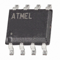
AT24HC04BN-SH-T Atmel, AT24HC04BN-SH-T Datasheet - Page 3

AT24HC04BN-SH-T
Manufacturer Part Number
AT24HC04BN-SH-T
Description
IC EEPROM 4KBIT 1MHZ 8SOIC
Manufacturer
Atmel
Datasheet
1.AT24HC04B-TH-B.pdf
(19 pages)
Specifications of AT24HC04BN-SH-T
Format - Memory
EEPROMs - Serial
Memory Type
EEPROM
Memory Size
4K (512 x 8)
Speed
400kHz, 1MHz
Interface
I²C, 2-Wire Serial
Voltage - Supply
1.8 V ~ 5.5 V
Operating Temperature
-40°C ~ 85°C
Package / Case
8-SOIC (3.9mm Width)
Density
4Kb
Interface Type
Serial (2-Wire)
Organization
512x8
Access Time (max)
900ns
Frequency (max)
400KHz
Write Protection
Yes
Data Retention
100Year
Operating Supply Voltage (typ)
2.5/3.3/5V
Package Type
SOIC
Operating Temp Range
-40C to 85C
Supply Current
3mA
Operating Supply Voltage (min)
1.8V
Operating Supply Voltage (max)
5.5V
Operating Temperature Classification
Industrial
Mounting
Surface Mount
Pin Count
8
Lead Free Status / RoHS Status
Lead free / RoHS Compliant
Available stocks
Company
Part Number
Manufacturer
Quantity
Price
Company:
Part Number:
AT24HC04BN-SH-T
Manufacturer:
Atmel
Quantity:
16 000
Company:
Part Number:
AT24HC04BN-SH-T
Manufacturer:
ATMEL
Quantity:
27
1. Pin Description
5227E–SEEPR–11/08
SERIAL CLOCK (SCL): The SCL input is used to positive edge clock data into each EEPROM
device and negative edge clock data out of each device.
SERIAL DATA (SDA): The SDA pin is bidirectional for serial data transfer. This pin is open-
drain driven and may be wire-ORed with any number of other open-drain or open collector
devices.
DEVICE/PAGE ADDRESSES (A2, A1, A0): The A2 and A1 pins are device address inputs that
must be hardwired for the AT24HC04B. As many as four 4K devices may be addressed on a
single bus system. The A0 pin is a no-connect. (Device addressing and Page addressing are
discussed in detail under Device Addressing and Page Addressing,
WRITE PROTECT (WP): The AT24HC04B has a WP pin that provides hardware data protec-
tion. The WP pin allows normal read/write operations when connected to ground (GND). When
the WP pin is connected to V
Table 1-1.
WP Pin Status
At V
At GND
CC
Write Protect
CC
, the write protection feature is enabled and operates as shown.
Normal Read/Write Operations
Part of the Array Protected
Upper Half (2K) Array
24HC04B
page
AT24HC04B
8).
3


