AT25128B-XHL-T Atmel, AT25128B-XHL-T Datasheet
AT25128B-XHL-T
Specifications of AT25128B-XHL-T
Available stocks


Related parts for AT25128B-XHL-T


AT25128B-XHL-T Summary of contents
Page 1
... SOIC, 8-lead TSSOP, 8-ball VFBGA and 8-lead UDFN pack- ages. In addition, the entire family is available in 1.8V (1.8V to 5.5V). The AT25128B/256B is enabled through the Chip Select pin (CS) and accessed via a 3-wire interface consisting of Serial Data Input (SI), Serial Data Output (SO), and Serial Clock (SCK) ...
Page 2
... Voltage on Any Pin with Respect to Ground.............................. –1.0 V +7.0V Maximum Operating Voltage................................. 6.25V DC Output Current .............................................. 5.0 mA Figure 1-1. Block Diagram AT25128B/256B 2 *NOTICE: Stresses beyond those listed under “Absolute Maximum Ratings” may cause permanent damage to the device. This is a stress rating only and functional operation of the device at ...
Page 3
... V = 5.0V 0°C to 70° 3 3.6V V 5. 1 0. 1.8V V 3. 100 µ AT25128B/256B = +5.0V (unless otherwise noted) CC Max Units Conditions OUT +1.8V to +5.5V, CC Min Typ Max 1.8 5.5 2.5 5.5 4.5 5.5 9.0 10.0 5.0 7.0 2.2 3.5 0.2 3.0 ...
Page 4
... Data In Setup Time SU t Data In Hold Time H t HOLD Setup Time HD t HOLD Hold Time CD t Output Valid V t Output Hold Time HO AT25128B/256B 4 = 40° 85°C, V – Voltage Min 4.5–5.5 0 2.5–5.5 0 1.8–5.5 0 4.5–5.5 2.5–5.5 1.8–5.5 4.5– ...
Page 5
... WP going low will have no effect on any write operation to the status register. The WP pin function is blocked when the WPEN bit in the status register is “0”. This will allow the user to install the AT25128B/256B in a system with the WP pin tied to ground and still be able to write to the status register. All WP pin functions are enabled when the WPEN bit is set to “ ...
Page 6
... Figure 2-1. SPI Serial Interface AT25128B/256B 6 AT25128B/256B 8698B–SEEPR–3/10 ...
Page 7
... Functional Description The AT25128B/256B is designed to interface directly with the synchronous serial peripheral interface (SPI) of the 6800 type series of microcontrollers. The AT25128B/256B utilizes an 8-bit instruction register. The list of instructions and their operation codes are con- tained in Table 3-1. All instructions, addresses, and data are transferred with the MSB first and start with a high-to- low CS transition ...
Page 8
... WRITE STATUS REGISTER (WRSR): The AT25128B/256B is divided into four array segments. Top quarter (1/4), top half (1/2), or all of the memory seg- ments can be protected. Any of the data within any selected segment will therefore be read only. The block write protection levels and corresponding status register control bits are shown in The three bits, BP0, BP1, and WPEN are nonvolatile cells that have the same properties and functions as the reg- ular memory cells (e ...
Page 9
... Bit the Write cycle is still in progress. If Bit the Write cycle has ended. Only the Read Status Register instruction is enabled during the Write programming cycle. The AT25128B/256B is capable of a 64-byte Page Write operation. After each byte of data is received, the six low order address bits are internally incremented by one; the high order bits of the address will remain constant. If more than 64 bytes of data are transmitted, the address counter will roll over and the previously written data will be overwritten ...
Page 10
... Timing Diagram (for SPI Mode 0 (0,0) Figure 4-1. Synchronous Data Timing CSS V IH SCK HI Figure 4-2. WREN Timing CS SCK SI SO Figure 4-3. WRDI Timing CS SCK SI SO AT25128B/256B VALID IN WREN OP-CODE HI-Z WRDI OP-CODE HI CSH t DIS HI-Z 8698B–SEEPR–3/10 ...
Page 11
... Figure 4-4. RDSR Timing SCK SI INSTRUCTION HIGH IMPEDANCE SO Figure 4-5. WRSR Timing SCK SI HIGH IMPEDANCE SO Figure 4-6. READ Timing SCK SI INSTRUCTION HIGH IMPEDANCE SO 8698B–SEEPR–3/ MSB INSTRUCTION BYTE ADDRESS ... A N AT25128B/256B DATA OUT DATA DATA OUT MSB 11 ...
Page 12
... Figure 4-7. WRITE Timing SCK SI INSTRUCTION HIGH IMPEDANCE SO Figure 4-8. HOLD Timing CS SCK HOLD SO AT25128B/256B BYTE ADDRESS ... DATA 8698B–SEEPR–3/10 ...
Page 13
... Ordering Code Detail Atmel Designator Product Family Device Density 128 = 128k 256 = 156k Device Revision 8698B–SEEPR–3/ AT25128B/256B Shipping Carrier Option B or blank = Bulk (tubes Tape and Reel Operating Voltage L = 1.8V to 5.5V Package Device Grade or Wafer/Die Thickness H = Green, NiPdAu lead finish, Industrial Temperature range (-40° ...
Page 14
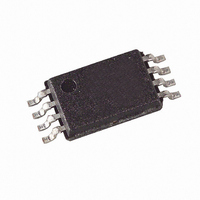
... PIN 1 INDICATOR (DOT) AT25128B-XHL Top Mark PIN 1 INDICATOR (DOT |---|---|---|---|---|---| A T |---|---|---|---|---|---| 5 D |---|---|---|---|---|---|---| ATMEL |---|---|---|---|---|---|---| AT25128B-MAHL Top Mark |---|---|---| 5 |---|---|---| H |---|---|---| Y |---|---|---| * | PIN 1 INDICATOR (DOT) AT25128B/256B 14 Seal Year | Seal Week @ = Country of Ass’ SEAL YEAR 6: 2006 2007 8: 2008 2009 @ = Country of Ass’ SEAL YEAR 8: 2008 2009 ...
Page 15
... Country of Ass’ SEAL YEAR 8: 2008 2009 0: 2010 2011 AT25128B/256B M = SEAL MONTH (USE ALPHA DESIGNATOR A- JANUARY B = FEBRUARY " " """""""" OCTOBER K = NOVEMBER L = DECEMBER WW = SEAL WEEK 0: 2010 02 = Week 2 1: 2011 04 = Week 4 2: 2012 ...
Page 16
... Y |---|---|---| * | PIN 1 INDICATOR (DOT) AT25256B-CUL Top Mark |---|---|---|---| |---|---|---|---| |---|---|---|---|---| * <-- PIN 1 INDICATOR AT25128B/256B YEAR OF ASSEMBLY Country of Ass’y XX= ATMEL LOT NUMBER TO COORESPOND L @ WITH TRACE CODE LOG BOOK. (e. AA, AB, AC,... AX, AY, AZ SEAL YEAR 6: 2006 7: 2007 8: 2008 9: 2009 B = Country of Origin Y = One Digit Year Code M = One Digit Month Code ...
Page 17
... AT25128B Ordering Information Ordering Code (1) AT25128B-SSHL-B (NiPdAu Lead Finish) (2) AT25128B-SSHL-T (NiPdAu Lead Finish) (1) AT25128B-XHL-B (NiPdAu Lead Finish) (2) AT25128B-XHL-T (NiPdAu Lead Finish) (2) AT25128B-MAHL-T (NiPdAu Lead Finish) (2) AT25128B-CUL-T (SnAgCu Ball Finish) (3) AT25128B-WWU11L Notes: 1. Bulk delivery in tubes (SOIC and TSSOP 100/tube). 2. Tape and reel delivery (SOIC 4k/reel. TSSOP, UDFN and VFBGA 5k/reel). ...
Page 18
... Wide, Plastic Gull Wing Small Outline Package (JEDEC SOIC) 8A2 8-lead, 0.170" Wide, Thin Shrink Small Outline Package (TSSOP) 8MA2 8-lead, 2.00mm x 3.00mm Body, 0.50 mm Pitch, Dual No Lead Package (UDFN) 8U2-1 8-ball, die Ball Grid Array Package (VFBGA) AT25128B/256B 18 Package Voltage Range 1.8V to 5.5V 8S1 8S1 1 ...
Page 19
... Top View Side View TITLE 8S1, 8-lead, (0.150” Wide Body), Plastic Gull Wing Outline (JEDEC SOIC) AT25128B/256B E1 L Ø End View COMMON DIMENSIONS (Unit of Measure = mm) SYMBOL MIN NOM MAX 1.75 A 1.35 – 0.25 A1 0.10 – b 0.31 – ...
Page 20
... Allowable Dambar protrusion shall be 0.08 mm total in excess of the b dimension at maximum material condition. Dambar cannot be located on the lower radius of the foot. Minimum space between protrusion and adjacent lead is 0.07 mm. 5. Dimension D and determined at Datum Plane H. Package Drawing Contact: packagedrawings@atmel.com AT25128B/256B End View D does not include ...
Page 21
... E 8 Pin Pin (R0.10) 0. TITLE 8MA2, 8-pad 0.6 mm Body, Thermally Enhanced Plastic Ultra Thin Dual Flat No Lead Package (UDFN) AT25128B/256B C COMMON DIMENSIONS (Unit of Measure = mm) SYMBOL MIN NOM MAX D 2.00 BSC E 3.00 BSC 1.60 D2 1.40 1.50 E2 1.20 1.30 1.40 A 0.50 0.55 ...
Page 22
... VFBGA A1 Ball Pad Corner e (e1) Notes: 1. This drawing is for general information. 2. Dimension 'b' is measured at the maximum solder ball diameter. 3. Solder ball composition shall be 95.5Sn-4.0Ag-.5Cu. Package Drawing Contact: packagedrawings@atmel.com AT25128B/256B 22 0.10 (4X Top View A1 BALL PAD CORNER (d1) Bottom View 8 SOLDER BALLS TITLE 8U2-1, 8 ball, 2 ...
Page 23
... Revision History Doc. Rev. Date 8698B 03/2010 8698A 12/2009 8698B–SEEPR–3/10 Comments Update Catalog Numbering Scheme. Update Ordering Information and package types. Initial document release. AT25128B/256B 23 ...
Page 24
... Disclaimer: The information in this document is provided in connection with Atmel products. No license, express or implied, by estoppel or otherwise, to any intellectual property right is granted by this document or in connection with the sale of Atmel products. EXCEPT AS SET FORTH IN ATMEL’S TERMS AND CONDI- TIONS OF SALE LOCATED ON ATMEL’S WEB SITE, ATMEL ASSUMES NO LIABILITY WHATSOEVER AND DISCLAIMS ANY EXPRESS, IMPLIED OR STATUTORY WARRANTY RELATING TO ITS PRODUCTS INCLUDING, BUT NOT LIMITED TO, THE IMPLIED WARRANTY OF MERCHANTABILITY, FITNESS FOR A PARTICULAR PURPOSE, OR NON-INFRINGEMENT ...