AT27C080-90PU Atmel, AT27C080-90PU Datasheet - Page 3
AT27C080-90PU
Manufacturer Part Number
AT27C080-90PU
Description
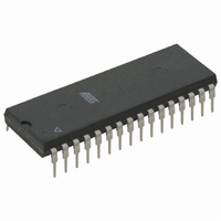
IC OTP 8MBIT 90NS 32DIP
Manufacturer
Atmel
Specifications of AT27C080-90PU
Format - Memory
EPROMs
Memory Type
OTP EPROM
Memory Size
8M (1M x 8)
Speed
90ns
Interface
Parallel
Voltage - Supply
4.5 V ~ 5.5 V
Operating Temperature
-40°C ~ 85°C
Package / Case
32-DIP (0.600", 15.24mm)
Capacitance, Input
4 pF
Capacitance, Output
8 pF
Current, Input, Leakage
±1 μA (Read)
Current, Operating
40 mA (Read)
Current, Output, Leakage
±5 μA (Read)
Density
8M
Organization
1M×8
Package Type
PDIP
Temperature, Operating
-40 to +85 °C
Time, Access
90 ns
Time, Address Setup
2
Time, Fall
20 ns
Time, Rise
20 ns
Voltage, Esd
2000 V
Voltage, Input, High
5.5 V (Read)
Voltage, Input, Low
0.8 V (Read)
Voltage, Output, High
2.4 V (Read)
Voltage, Output, Low
0.4 V (Read)
Voltage, Supply
5 V
Access Time
90ns
Supply Voltage Range
4.5V To 5.5V
No. Of Pins
32
Operating Temperature Range
-40°C To +85°C
Ic Interface Type
Parallel
Supply Voltage Max
5.5V
Rohs Compliant
Yes
Operating Temperature Max
85°C
Memory Configuration
1M X 8
Memory Case Style
DIP
Lead Free Status / RoHS Status
Lead free / RoHS Compliant
Available stocks
Company
Part Number
Manufacturer
Quantity
Price
Company:

Part Number:
AT27C080-90PU
Manufacturer:
TI
Quantity:
3 400
Part Number:
AT27C080-90PU
Manufacturer:
ATMEL
Quantity:
20 000


3. System Considerations
4. Block Diagram
5. Absolute Maximum Ratings*
Note:
0360L–EPROM–12/07
Temperature Under Bias................................ -55°C to +125°C
Storage Temperature ..................................... -65°C to +150°C
Voltage on Any Pin with
Respect to Ground .........................................-2.0V to +7.0V
Voltage on A9 with
Respect to Ground ......................................-2.0V to +14.0V
V
Respect to Ground .......................................-2.0V to +14.0V
Integrated UV Erase Dose............................. 7258 W•sec/cm
PP
Supply Voltage with
1. Minimum voltage is -0.6V DC which may undershoot to -2.0V for pulses of less than 20 ns. Maximum output pin voltage is
V
CC
+ 0.75V DC which may overshoot to +7.0V for pulses of less than 20 ns.
Switching between active and standby conditions via the Chip Enable pin may produce tran-
sient voltage excursions. Unless accommodated by the system design, these transients may
exceed datasheet limits, resulting in device non-conformance. At a minimum, a 0.1 µF high
frequency, low inherent inductance, ceramic capacitor should be utilized for each device. This
capacitor should be connected between the V
to the device as possible. Additionally, to stabilize the supply voltage level on printed circuit
boards with large EPROM arrays, a 4.7 µF bulk electrolytic capacitor should be utilized, again
connected between the V
close as possible to the point where the power supply is connected to the array.
CC
(1)
(1)
(1)
2
and Ground terminals. This capacitor should be positioned as
*NOTICE:
CC
Stresses beyond those listed under “Absolute
Maximum Ratings” may cause permanent
damage to the device. This is a stress rating
only and functional operation of the device at
these or any other conditions beyond those
indicated in the operational sections of this
specification is not implied. Exposure to abso-
lute maximum rating conditions for extended
periods may affect device reliability.
and Ground terminals of the device, as close
AT27C080
3
Related parts for AT27C080-90PU
Image
Part Number
Description
Manufacturer
Datasheet
Request
R

Part Number:
Description:
IC OTP 8MBIT 120NS 32PLCC
Manufacturer:
Atmel
Datasheet:

Part Number:
Description:
IC OTP 8MBIT 90NS 32DIP
Manufacturer:
Atmel
Datasheet:
Part Number:
Description:
IC OTP 8MBIT 120NS 32DIP
Manufacturer:
Atmel
Datasheet:
Part Number:
Description:
IC OTP 8MBIT 120NS 32DIP
Manufacturer:
Atmel
Datasheet:

Part Number:
Description:
IC OTP 8MBIT 150NS 32TSOP
Manufacturer:
Atmel
Datasheet:
Part Number:
Description:
IC OTP 8MBIT 90NS 32PLCC
Manufacturer:
Atmel
Datasheet:
Part Number:
Description:
IC OTP 8MBIT 90NS 32DIP
Manufacturer:
Atmel
Datasheet:
Part Number:
Description:
IC OTP 8MBIT 90NS 32TSOP
Manufacturer:
Atmel
Datasheet:
Part Number:
Description:
IC OTP 8MBIT 90NS 32PLCC
Manufacturer:
Atmel
Datasheet:

Part Number:
Description:
IC EPROM 8MBIT 120NS 32CDIP
Manufacturer:
Atmel
Datasheet:
Part Number:
Description:
IC EPROM 8MBIT 90NS 32CDIP
Manufacturer:
Atmel
Datasheet:
Part Number:
Description:
IC OTP 8MBIT 90NS 32PLCC
Manufacturer:
Atmel
Datasheet:
Part Number:
Description:
IC OTP 8MBIT 120NS 32PLCC
Manufacturer:
Atmel
Datasheet:

Part Number:
Description:
IC OTP 8MBIT 120NS 32SOIC
Manufacturer:
Atmel
Datasheet:
Part Number:
Description:
IC OTP 8MBIT 120NS 32SOIC
Manufacturer:
Atmel
Datasheet: