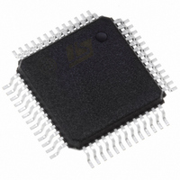
PSD834F2-70M STMicroelectronics, PSD834F2-70M Datasheet - Page 63

PSD834F2-70M
Manufacturer Part Number
PSD834F2-70M
Description
IC FLASH 2MBIT 70NS 52QFP
Manufacturer
STMicroelectronics
Datasheet
1.PSD813F2VA-20JI.pdf
(109 pages)
Specifications of PSD834F2-70M
Format - Memory
FLASH
Memory Type
FLASH
Memory Size
2M (256K x 8)
Speed
70ns
Interface
Parallel
Voltage - Supply
4.5 V ~ 5.5 V
Operating Temperature
0°C ~ 70°C
Package / Case
52-QFP
Lead Free Status / RoHS Status
Contains lead / RoHS non-compliant
Other names
497-2005
Available stocks
Company
Part Number
Manufacturer
Quantity
Price
Company:
Part Number:
PSD834F2-70M
Manufacturer:
Samsung
Quantity:
6 000
Company:
Part Number:
PSD834F2-70M
Manufacturer:
STMicroelectronics
Quantity:
10 000
Automatic Power-down (APD) Unit and Power-down Mode
The APD Unit, shown in Figure 32, puts the PSD
into Power-down mode by monitoring the activity
of Address Strobe (ALE/AS, PD0). If the APD Unit
is enabled, as soon as activity on Address Strobe
(ALE/AS, PD0) stops, a four bit counter starts
counting. If Address Strobe (ALE/AS, PD0) re-
mains inactive for fifteen clock periods of CLKIN
(PD1), Power-down (PDN) goes High, and the
PSD enters Power-down mode, as discussed
next.
Power-down Mode. By default, if you enable the
APD Unit, Power-down mode is automatically en-
abled. The device enters Power-down mode if Ad-
dress Strobe (ALE/AS, PD0) remains inactive for
fifteen periods of CLKIN (PD1).
The following should be kept in mind when the
PSD is in Power-down mode:
–
–
–
Figure 32. APD Unit
Table 29. PSD Timing and Standby Current during Power-down Mode
Note: 1. Power-down does not affect the operation of the PLD. The PLD operation in this mode is based only on the Turbo Bit.
Power-down
Mode
If Address Strobe (ALE/AS, PD0) starts
pulsing again, the PSD returns to normal
Operating mode. The PSD also returns to
normal Operating mode if either PSD Chip
Select Input (CSI, PD2) is Low or the Reset
(RESET) input is High.
The MCU address/data bus is blocked from all
memory and PLDs.
Various signals can be blocked (prior to
Power-down mode) from entering the PLDs by
setting the appropriate bits in the PMMR
2. Typical current consumption assuming no PLD inputs are changing state and the PLD Turbo Bit is ’0.’
PLD Propagation Delay
Normal t
APD EN
PMMR0 BIT 1=1
ALE
RESET
CSI
CLKIN
PD
(Note
DISABLE
FLASH/EEPROM/SRAM
TRANSITION
DETECTION
DETECT
1
EDGE
)
Access Time
No Access
Memory
Doc ID 10552 Rev 3
CLR
COUNTER
APD
PD
PD
Access Recovery Time
–
–
Table 28. Power-down Mode’s Effect on Ports
to Normal Access
MCU I/O
PLD Out
Address Out
Data Port
Peripheral I/O
DISABLE BUS
INTERFACE
registers. The blocked signals include MCU
control signals and the common CLKIN (PD1).
Note that blocking CLKIN (PD1) from the
PLDs does not block CLKIN (PD1) from the
APD Unit.
All PSD memories enter standby mode and
are drawing standby current. However, the
PLD and I/O ports blocks do not go into
standby Mode because you don’t want to have
to wait for the logic and I/O to “wake-up”
before their outputs can change. See Table
for Power-down mode effects on PSD ports.
Typical standby current is of the order of
microamperes. These standby current values
assume that there are no transitions on any
PLD input.
Port Function
t
LVDV
PLD
EEPROM SELECT
FLASH SELECT
POWER DOWN
( PDN )
SRAM SELECT
SELECT
PSD813F2V, PSD854F2V
75µA (Note
Typical Standby Current
5V V
No Change
No Change
Undefined
Tri-State
Tri-State
CC
AI02891
Pin Level
2
)
25µA (Note
3V V
CC
63/109
28
2
)


