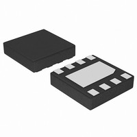
CAT25080HU2I-GT3 ON Semiconductor, CAT25080HU2I-GT3 Datasheet - Page 10

CAT25080HU2I-GT3
Manufacturer Part Number
CAT25080HU2I-GT3
Description
IC EEPROM 8KB SPI SER 8UDFN
Manufacturer
ON Semiconductor
Datasheet
1.CAT25080YI-GT3.pdf
(16 pages)
Specifications of CAT25080HU2I-GT3
Format - Memory
EEPROMs - Serial
Memory Type
EEPROM
Memory Size
8K (1K x 8)
Speed
10MHz
Interface
SPI, 3-Wire Serial
Voltage - Supply
1.8 V ~ 5.5 V
Operating Temperature
-40°C ~ 85°C
Package / Case
8-UFDFN Exposed Pad
Lead Free Status / RoHS Status
Lead free / RoHS Compliant
Available stocks
Company
Part Number
Manufacturer
Quantity
Price
Company:
Part Number:
CAT25080HU2I-GT3
Manufacturer:
ON Semiconductor
Quantity:
2 400
Part Number:
CAT25080HU2I-GT3
Manufacturer:
ON/安森美
Quantity:
20 000
Hold Operation
between host and CAT25080/160. To pause, HOLD must be
taken low while SCK is low (Figure 11). During the hold
condition the device must remain selected (CS low). During
the pause, the data output pin (SO) is tri−stated (high
impedance) and SI transitions are ignored. To resume
communication, HOLD must be taken high while SCK is low.
Design Considerations
(POR) circuitry which protects the internal logic against
powering up in the wrong state. The device will power up
into Standby mode after V
and will power down into Reset mode when V
The HOLD input can be used to pause communication
The CAT25080/160 devices incorporate Power−On Reset
HOLD
SCK
CS
SO
Dashed Line = mode (1, 1)
CC
exceeds the POR trigger level
t
HD
t
CD
t
HZ
Figure 11. HOLD Timing
CC
http://onsemi.com
drops
10
HIGH IMPEDANCE
below the POR trigger level. This bi−directional POR
behavior protects the device against ‘brown−out’ failure
following a temporary loss of power.
state and in a low power standby mode. A WREN instruction
must be issued prior to any writes to the device.
a ready state and receive an instruction. After a successful
byte/page write or status register write, the device goes into
a write disable mode. The CS input must be set high after the
proper number of clock cycles to start the internal write
cycle. Access to the memory array during an internal write
cycle is ignored and programming is continued. Any invalid
op−code will be ignored and the serial output pin (SO) will
remain in the high impedance state.
The CAT25080/160 device powers up in a write disable
After power up, the CS pin must be brought low to enter
t
HD
t
CD
t
LZ


