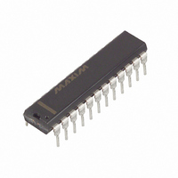
DS1220Y-200IND+ Maxim Integrated Products, DS1220Y-200IND+ Datasheet

DS1220Y-200IND+
Specifications of DS1220Y-200IND+
Related parts for DS1220Y-200IND+
DS1220Y-200IND+ Summary of contents
Page 1
... The NV SRAM can be used in place of existing SRAMs directly conforming to the popular bytewide 24-pin DIP standard. The DS1220Y also matches the pinout of the 2716 EPROM or the 2816 EEPROM, allowing direct substitution while enhancing performance. There is no limit on the number of write cycles that can be executed and no additional support circuitry is required for microprocessor interfacing ...
Page 2
... OE WRITE MODE The DS1220Y executes a write cycle whenever the WE and CE signals are active (low) after address inputs are stable. The later-occurring falling edge will determine the start of the write cycle. The write cycle is terminated by the earlier rising edge All address inputs must be kept valid throughout the write cycle ...
Page 3
... SYMBOL MIN TYP I -0.3V to +6.0V 0°C to +70°C -40°C to +85°C -40°C to +85°C +260° See Note 10) A MAX UNITS NOTES 5 ± 10%) CC MAX UNITS NOTES µA +1.0 µA +1 3.0 7.0 mA 2.0 4 +25°C) A MAX UNITS NOTES DS1220Y ...
Page 4
... Output High-Z from WE Output Active from WE Data Setup Time Data Hold Time (T : See Note 10 DS1220Y-100 SYM MIN MAX t 100 RC t 100 ACC 100 COE 100 WR1 t 10 WR2 t 35 ODW t 5 OEW DH1 t 10 DH2 DS1220Y = 5.0V ± 10%) CC UNITS NOTES ...
Page 5
... NOT RECOMMENDED FOR NEW DESIGNS READ CYCLE SEE NOTE 1 WRITE CYCLE 1 SEE NOTES AND 12 WRITE CYCLE 2 SEE NOTES AND DS1220Y ...
Page 6
... These parameters are sampled with load and are not 100% tested. SYMBOL MIN 100 REC SYMBOL MIN during a write cycle, the output buffers remain in a high impedance IH is measured from the latter DS1220Y MAX UNITS NOTES µs µs µ +25°C) A MAX UNITS NOTES years 11 9 ...
Page 7
... low or the WE low transition occurs prior to or simultaneously with the CE low transition, the output buffers remain in a high impedance state during this period. 9. Each DS1220Y is marked with a 4-digit date code AABB. AA designates the year of manufacture. BB designates the week of manufacture. The expected t manufacture ...
Page 8
... PACKAGE CODE 24 DIP OUTLINE NO. MDT24+3 21-0245 PKG DIM DS1220Y LAND PATTERN NO. 24-PIN MIN MAX 1.320 1.340 33.53 34.04 0.695 0.720 17.65 18.29 0.390 0.415 9.91 10.54 0.100 0.130 2.54 3.30 0.017 0.030 0.43 0.76 0.120 ...
Page 9
... Maximr cannot assume responsibility for use of any circuitry other than circuitry entirely embodied in a Maxim product. No circuit patent licenses are implied. Maxim reserves the right to change the circuitry and specifications without notice at any time © 2010 Maxim Integrated Products DESCRIPTION Maxim and the Dallas logos are registered trademarks of Maxim Integrated Products, Inc. DS1220Y PAGES CHANGED ...


