DS1230YP-70 Maxim Integrated Products, DS1230YP-70 Datasheet - Page 2
DS1230YP-70
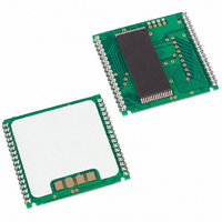
Manufacturer Part Number
DS1230YP-70
Description
IC NVSRAM 256KBIT 70NS 34PCM
Manufacturer
Maxim Integrated Products
Datasheet
1.DS1230Y-150.pdf
(10 pages)
Specifications of DS1230YP-70
Format - Memory
RAM
Memory Type
NVSRAM (Non-Volatile SRAM)
Memory Size
256K (32K x 8)
Speed
70ns
Interface
Parallel
Voltage - Supply
4.5 V ~ 5.5 V
Operating Temperature
0°C ~ 70°C
Package / Case
34-PowerCap™ Module
Lead Free Status / RoHS Status
Contains lead / RoHS non-compliant
Available stocks
Company
Part Number
Manufacturer
Quantity
Price

Part Number:
DS1230YP-70
Manufacturer:
DALLAS
Quantity:
20 000
Company:
Part Number:
DS1230YP-70+
Manufacturer:
Maxim Integrated Products
Quantity:
135


DESCRIPTION
The DS1230 256k Nonvolatile SRAMs are 262,144-bit, fully static, nonvolatile SRAMs organized as
32,768 words by 8 bits. Each NV SRAM has a self-contained lithium energy source and control circuitry
which constantly monitors V
lithium energy source is automatically switched on and write protection is unconditionally enabled to
prevent data corruption. DIP-package DS1230 devices can be used in place of existing 32k x 8 static
RAMs directly conforming to the popular bytewide 28-pin DIP standard. The DIP devices also match the
pinout of 28256 EEPROMs, allowing direct substitution while enhancing performance. DS1230 devices
in the Low Profile Module package are specifically designed for surface-mount applications. There is no
limit on the number of write cycles that can be executed and no additional support circuitry is required for
microprocessor interfacing.
READ MODE
The DS1230 devices execute a read cycle whenever
Enable) and
(A
eight data output drivers within t
that
satisfied, then data access must be measured from the later-occurring signal (
parameter is either t
WRITE MODE
The DS1230 devices execute a write cycle whenever the
address inputs are stable. The later-occurring falling edge of
write cycle. The write cycle is terminated by the earlier rising edge of
be kept valid throughout the write cycle.
(t
write cycles to avoid bus contention. However, if the output drivers are enabled (
DATA RETENTION MODE
The DS1230AB provides full functional capability for V
4.5 volts. The DS1230Y provides full functional capability for V
protects by 4.25 volts. Data is maintained in the absence of V
The nonvolatile static RAMs constantly monitor V
automatically write protect themselves, all inputs become “don’t care,” and all outputs become high-
impedance. As V
energy source to RAM to retain data. During power-up, when V
the power switching circuit connects external V
Normal RAM operation can resume after V
DS1230Y.
FRESHNESS SEAL
Each DS1230 device is shipped from Maxim with its lithium energy source disconnected, guaranteeing
full energy capacity. When V
is enabled for battery back-up operation.
WE
WR
0
- A
) before another cycle can be initiated. The
will disable the outputs in t
CE
14
) defines which of the 32,768 bytes of data is to be accessed. Valid data will be available to the
and
OE
OE
(Output Enable) are active (low). The unique address specified by the 15 address inputs
CC
(Output Enable) access times are also satisfied. If
CO
falls below approximately 3.0 volts, a power switching circuit connects the lithium
for
CE
CC
CC
or t
ODW
is first applied at a level greater than 4.25 volts, the lithium energy source
ACC
for an out-of-tolerance condition. When such a condition occurs, the
OE
from its falling edge.
for
(Access Time) after the last address input signal is stable, providing
OE
WE
CC
rather than address access.
must return to the high state for a minimum recovery time
exceeds 4.75 volts for the DS1230AB and 4.5 volts for the
2 of 10
OE
CC
CC
to RAM and disconnects the lithium energy source.
control signal should be kept inactive (high) during
WE
. Should the supply voltage decay, the NV SRAMs
CC
(Write Enable) is inactive (high) and
greater than 4.75 volts and write protects by
WE
CC
CE
without any additional support circuitry.
and
CC
or
CC
rises above approximately 3.0 volts
CE
WE
CE
OE
greater than 4.5 volts and write
or
will determine the start of the
signals are active (low) after
and
WE
CE
CE
. All address inputs must
or
CE
access times are not
OE
and
) and the limiting
OE
DS1230Y/AB
active) then
CE
(Chip
Related parts for DS1230YP-70
Image
Part Number
Description
Manufacturer
Datasheet
Request
R


Part Number:
Description:
IC NVSRAM 256KBIT 150NS 28DIP
Manufacturer:
Maxim Integrated Products
Datasheet:
Part Number:
Description:
IC NVSRAM 256KBIT 120NS 28DIP
Manufacturer:
Maxim Integrated Products
Datasheet:
Part Number:
Description:
IC NVSRAM 256KBIT 200NS 28DIP
Manufacturer:
Maxim Integrated Products
Datasheet:
Part Number:
Description:
IC NVSRAM 256KBIT 100NS 28DIP
Manufacturer:
Maxim Integrated Products
Datasheet:
Part Number:
Description:
IC NVSRAM 256KBIT 200NS 28DIP
Manufacturer:
Maxim Integrated Products
Datasheet:
Part Number:
Description:
IC NVSRAM 256KBIT 100NS 28DIP
Manufacturer:
Maxim Integrated Products
Datasheet:
Part Number:
Description:
IC NVSRAM 256KBIT 70NS 28DIP
Manufacturer:
Maxim Integrated Products
Datasheet:
Part Number:
Description:
IC NVSRAM 256KBIT 70NS 28DIP
Manufacturer:
Maxim Integrated Products
Datasheet:
Part Number:
Description:
IC NVSRAM 256KBIT 200NS 28DIP
Manufacturer:
Maxim Integrated Products
Datasheet:
Part Number:
Description:
IC NVSRAM 256KBIT 120NS 28DIP
Manufacturer:
Maxim Integrated Products
Datasheet:
Part Number:
Description:
IC NVSRAM 256KBIT 70NS 28DIP
Manufacturer:
Maxim Integrated Products
Datasheet:
Part Number:
Description:
IC NVSRAM 256KBIT 120NS 28DIP
Manufacturer:
Maxim Integrated Products
Datasheet:
Part Number:
Description:
IC NVSRAM 256KBIT 150NS 28DIP
Manufacturer:
Maxim Integrated Products
Datasheet:
Part Number:
Description:
IC NVSRAM 256KBIT 120NS 28DIP
Manufacturer:
Maxim Integrated Products
Datasheet: