DS1230YP-70 Maxim Integrated Products, DS1230YP-70 Datasheet - Page 8
DS1230YP-70
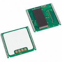
Manufacturer Part Number
DS1230YP-70
Description
IC NVSRAM 256KBIT 70NS 34PCM
Manufacturer
Maxim Integrated Products
Datasheet
1.DS1230Y-150.pdf
(10 pages)
Specifications of DS1230YP-70
Format - Memory
RAM
Memory Type
NVSRAM (Non-Volatile SRAM)
Memory Size
256K (32K x 8)
Speed
70ns
Interface
Parallel
Voltage - Supply
4.5 V ~ 5.5 V
Operating Temperature
0°C ~ 70°C
Package / Case
34-PowerCap™ Module
Lead Free Status / RoHS Status
Contains lead / RoHS non-compliant
Available stocks
Company
Part Number
Manufacturer
Quantity
Price

Part Number:
DS1230YP-70
Manufacturer:
DALLAS
Quantity:
20 000
Company:
Part Number:
DS1230YP-70+
Manufacturer:
Maxim Integrated Products
Quantity:
135


WARNING:
Under no circumstance are negative undershoots, of any amplitude, allowed when device is in battery
backup mode.
NOTES:
1.
2.
3. t
4. t
5. These parameters are sampled with a 5 pF load and are not 100% tested.
6. If the
7. If the
8. If
9. Each DS1230 has a built-in switch that disconnects the lithium source until the user first applies V
10. All AC and DC electrical characteristics are valid over the full operating temperature range. For
11. In a power-down condition the voltage on any pin may not exceed the voltage on V
12. t
13. t
14. DS1230 modules are recognized by Underwriters Laboratories (UL) under file E99151.
DC TEST CONDITIONS
Outputs Open
Cycle = 200 ns for operating current
All voltages are referenced to ground
PARAMETER
Expected Data Retention Time
going low to the earlier of
buffers remain in a high-impedance state during this period.
buffers remain in high-impedance state during this period.
the output buffers remain in a high-impedance state during this period.
The expected t
is first applied by the user. This parameter is assured by component selection, process control, and
design. It is not measured directly during production testing.
commercial products, this range is 0°C to 70°C. For industrial products (IND), this range is -40°C to
+85°C.
WE
OE
WP
DH
WR1
WR2
WE
, t
= V
is specified as the logical AND of
is high for a Read Cycle.
and t
and t
DS
CE
CE
is low or the
are measured from the earlier of
IH
DH1
DH2
or V
low transition occurs simultaneously with or latter than the
high transition occurs prior to or simultaneously with the
are measured from
are measured from
IL
DR
. If
is defined as accumulative time in the absence of V
OE
WE
= V
low transition occurs prior to or simultaneously with the
CE
IH
during write cycle, the output buffers remain in a high-impedance state.
or
CE
WE
WE
going high.
going high.
going high.
SYMBOL
CE
CE
t
or
and
DR
8 of 10
WE
AC TEST CONDITIONS
Output Load: 100 pF + 1TTL Gate
Input Pulse Levels: 0 - 3.0V
Timing Measurement Reference Levels
Input pulse Rise and Fall Times: 5 ns
WE
going high.
. t
MIN
WP
10
Input: 1.5V
Output: 1.5V
is measured from the latter of
TYP
CC
WE
WE
MAX
starting from the time power
high transition, the output
low transition, the output
UNITS
CC
CE
years
.
(T
low transition,
A
DS1230Y/AB
= +25°C)
CE
NOTES
or
9
WE
CC
.
Related parts for DS1230YP-70
Image
Part Number
Description
Manufacturer
Datasheet
Request
R


Part Number:
Description:
IC NVSRAM 256KBIT 150NS 28DIP
Manufacturer:
Maxim Integrated Products
Datasheet:
Part Number:
Description:
IC NVSRAM 256KBIT 120NS 28DIP
Manufacturer:
Maxim Integrated Products
Datasheet:
Part Number:
Description:
IC NVSRAM 256KBIT 200NS 28DIP
Manufacturer:
Maxim Integrated Products
Datasheet:
Part Number:
Description:
IC NVSRAM 256KBIT 100NS 28DIP
Manufacturer:
Maxim Integrated Products
Datasheet:
Part Number:
Description:
IC NVSRAM 256KBIT 200NS 28DIP
Manufacturer:
Maxim Integrated Products
Datasheet:
Part Number:
Description:
IC NVSRAM 256KBIT 100NS 28DIP
Manufacturer:
Maxim Integrated Products
Datasheet:
Part Number:
Description:
IC NVSRAM 256KBIT 70NS 28DIP
Manufacturer:
Maxim Integrated Products
Datasheet:
Part Number:
Description:
IC NVSRAM 256KBIT 70NS 28DIP
Manufacturer:
Maxim Integrated Products
Datasheet:
Part Number:
Description:
IC NVSRAM 256KBIT 200NS 28DIP
Manufacturer:
Maxim Integrated Products
Datasheet:
Part Number:
Description:
IC NVSRAM 256KBIT 120NS 28DIP
Manufacturer:
Maxim Integrated Products
Datasheet:
Part Number:
Description:
IC NVSRAM 256KBIT 70NS 28DIP
Manufacturer:
Maxim Integrated Products
Datasheet:
Part Number:
Description:
IC NVSRAM 256KBIT 120NS 28DIP
Manufacturer:
Maxim Integrated Products
Datasheet:
Part Number:
Description:
IC NVSRAM 256KBIT 150NS 28DIP
Manufacturer:
Maxim Integrated Products
Datasheet:
Part Number:
Description:
IC NVSRAM 256KBIT 120NS 28DIP
Manufacturer:
Maxim Integrated Products
Datasheet: