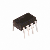
AT25040-10PC-2.7 Atmel, AT25040-10PC-2.7 Datasheet

AT25040-10PC-2.7
Specifications of AT25040-10PC-2.7
Related parts for AT25040-10PC-2.7
AT25040-10PC-2.7 Summary of contents
Page 1
... Serial Data Input SO Serial Data Output GND Ground VCC Power Supply WP Write Protect HOLD Suspends Serial Input 8-lead PDIP VCC HOLD SCK GND 8-lead SOIC VCC HOLD SCK GND SPI Serial EEPROMs 1K (128 (256 (512 x 8) AT25010 AT25020 AT25040 Rev. 0606M–SEEPR–06/03 1 ...
Page 2
Absolute Maximum Ratings* Operating Temperature................................. -55° 125°C Storage Temperature .................................... -65° 150°C Voltage on Any Pin with Respect to Ground ....................................-1. 7.0V Maximum Operating Voltage .......................................... 6.25V DC Output Current........................................................ 5.0 mA Block Diagram ...
Page 3
... OH1 V Output Low Voltage OL2 2.7V V Output High Voltage OH2 Note: 1. This parameter is preliminary and Atmel may change the specifications upon further characterization min and V max are reference only and are not tested 0606M–SEEPR–06/03 = 25° 1.0 MHz -40°C to +85° ...
Page 4
AC Characteristics Applicable over recommended operating range from T 100 pF (unless otherwise noted). Symbol Parameter f SCK Clock Frequency SCK t Input Rise Time RI t Input Fall Time FI t SCK High Time WH t SCK Low Time ...
Page 5
Serial Interface MASTER: The device that generates the serial clock. Description SLAVE: Because the Serial Clock pin (SCK) is always an input, the AT25010/020/040 always operates as a slave. TRANSMITTER/RECEIVER: The AT25010/020/040 has separate pins designated for data transmission (SO) ...
Page 6
... X001 READ 0000 A011 WRITE 0000 A010 Note: “A” represents MSB address bit A8. Operation Set Write Enable Latch Reset Write Enable Latch Read Status Register Write Status Register Read Data from Memory Array Write Data to Memory Array 0606M–SEEPR–06/03 ...
Page 7
... Bits 0-7 are 1s during an internal write cycle. Status Register Bits Level BP1 BP0 (1/ (1/ (All AT25010/020/040 Bit 3 Bit 2 Bit 1 X BP1 BP0 WEN , RDSR). WC Array Addresses Protected AT25010 AT25020 None None 60-7F C0-FF 40-7F 80-FF 00-7F 00-FF CC Bit 0 RDY AT25040 None 180-1FF 100-1FF 000-1FF 7 ...
Page 8
... READ sequence can be continued since the byte address is automatically incremented and data will continue to be shifted out. When the highest address is reached, the address counter will roll over to the lowest address allowing the entire memory to be read in one continuous READ cycle. ...
Page 9
Timing Diagrams Synchronous Data Timing (for mode CSS V IH SCK HI WREN Timing WRDI Timing 0606M–SEEPR–06/ ...
Page 10
RDSR Timing CS 0 SCK SI HIGH IMPEDANCE SO WRSR Timing CS 0 SCK SI HIGH IMPEDANCE SO READ Timing AT25010/020/040 INSTRUCTION 7 MSB ...
Page 11
WRITE Timing SCK INSTRUCTION SI HIGH IMPEDANCE SO HOLD Timing CS SCK HOLD SO 0606M–SEEPR–06/ BYTE ...
Page 12
AT25010 Ordering Information Ordering Code AT25010-10PI-2.7 AT25010N-10SI-2.7 Note: For 2.7V devices used in the 4.5V to 5.5V range, please refer to performance values in the AC and DC Characteristics tables. 8P3 8-lead, 0.300" Wide, Plastic Dual Inline Package (PDIP) 8S1 ...
Page 13
AT25020 Ordering Information Ordering Code AT25020-10PI-2.7 AT25020N-10SI-2.7 Note: For 2.7V devices used in the 4.5V to 5.5V range, please refer to performance values in the AC and DC Characteristics tables. 8P3 8-lead, 0.300" Wide, Plastic Dual Inline Package (PDIP) 8S1 ...
Page 14
... AT25040 Ordering Information Ordering Code AT25040-10PI-2.7 AT25040N-10SI-2.7 Note: For 2.7V devices used in the 4.5V to 5.5V range, please refer to performance values in the AC and DC Characteristics tables. 8P3 8-lead, 0.300" Wide, Plastic Dual Inline Package (PDIP) 8S1 8-lead, 0.150" Wide, Plastic Gull Wing Small Outline Package (JEDEC SOIC) -2 ...
Page 15
Packaging Information 8P3 – PDIP Top View PLCS Side View Notes: 1. This drawing is for general information only; refer to JEDEC Drawing MS-001, Variation BA for additional information. 2. Dimensions A and L are measured ...
Page 16
JEDEC SOIC 3 Top View e D Side View End View Note: This drawing is for general information only. Refer to JEDEC Drawing MS-012 for proper dimensions, tolerances, datums, etc. 2325 Orchard Parkway San Jose, ...
Page 17
... No licenses to patents or other intellectual property of Atmel are granted by the Company in connection with the sale of Atmel products, expressly or by implication. Atmel’s products are not authorized for use as critical components in life support devices or systems. ...


