AT25040A-10PI-1.8 Atmel, AT25040A-10PI-1.8 Datasheet
AT25040A-10PI-1.8
Specifications of AT25040A-10PI-1.8
AT25040-10PI-1.8


Related parts for AT25040A-10PI-1.8


AT25040A-10PI-1.8 Summary of contents
Page 1
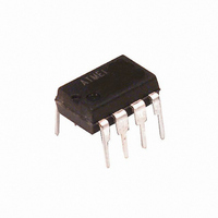
... TSSOP packages. 8-lead PDIP VCC HOLD SCK GND 8-lead Ultra Thin mini-MAP (MLP 2x3) 8-lead TSSOP VCC HOLD SCK GND Bottom view SPI Serial EEPROM 1K (128x8) 2K (256x8) 4K (512x8) AT25010A AT25020A AT25040A Not Recommended for New Design 8-lead SOIC 3348J–SEEPR–8/06 ...
Page 2
... This is a stress rating only and functional operation of the device at these or any other conditions beyond those indicated in the operational sections of this specification is not implied. Exposure to absolute maximum rating conditions for extended periods may affect device reliability. MEMORY ARRAY ADDRESS 128/256/512 X 8 DECODER DATA REGISTER MODE ...
Page 3
Table 2. Pin Capacitance Applicable over recommended operating range from T Symbol Test Conditions C Output Capacitance (SO) OUT C Input Capacitance (CS, SCK, SI, WP, HOLD) IN Note: 1. This parameter is characterized and is not 100% tested. ...
Page 4
Table 4. AC Characteristics Applicable over recommended operating range from TTL Gate and 30 pF (unless otherwise noted) Symbol Parameter f SCK Clock Frequency SCK t Input Rise Time RI t Input Fall Time FI t ...
Page 5
Table 4. AC Characteristics (Continued) Applicable over recommended operating range from TTL Gate and 30 pF (unless otherwise noted) Symbol Parameter t Hold to Output Low Hold to Output High ...
Page 6
Serial Interface Description AT25010A/020A/040A 6 MASTER: The device that generates the serial clock ...
Page 7
Figure 2. SPI Serial Interface AT25010A/020A/040A AT25010A/020A/040A 7 ...
Page 8
... Bits 0–7 are “1”s during an internal write cycle. WRITE STATUS REGISTER (WRSR): The WRSR instruction allows the user to select one of four levels of protection. The AT25010A/020A/040A is divided into four array seg- ments. One-quarter, one-half, or all of the memory segments can be protected. Any of Operation Set Write Enable Latch ...
Page 9
... Write instruction and will return to the standby state, when CS is brought high. A new CS falling edge is required to reinitiate the serial communication. AT25010A/020A/040A , RDSR). WC Array Addresses Protected AT25010A AT25020A None None 607F C0FF 407F 80FF 007F 00FF AT25040A None 180FF 1001FF 0001FF 9 ...
Page 10
Timing Diagrams Figure 3. Synchronous Data Timing (for Mode CSS V IH SCK HI Figure 4. WREN Timing Figure ...
Page 11
Figure 6. RDSR Timing SCK INSTRUCTION SI HIGH IMPEDANCE SO Figure 7. WRSR Timing SCK INSTRUCTION SI HIGH IMPEDANCE SO Figure 8. READ Timing 3348J–SEEPR–8/ MSB ...
Page 12
Figure 9. WRITE Timing SCK INSTRUCTION SI HIGH IMPEDANCE SO Figure 10. HOLD Timing CS SCK HOLD SO AT25010A/020A/040A 12 BYTE ADDRESS 8 7 ...
Page 13
AT25010A Ordering Information Ordering Code (2) AT25010A-10PU-2.7 (2) AT25010A-10PU-1.8 (2) AT25010AN-10SU-2.7 (2) AT25010AN-10SU-1.8 (2) AT25010A-10TU-2.7 (2) AT25010A-10TU-1.8 (2) AT25010AY1-10YU-1.8 (Not recommended for new designs) (3) AT25010AY6-10YH-1.8 (4) AT25010A-W1.8-11 Notes: 1. For 2.7V devices used in the 4.5 to 5.5V range, ...
Page 14
AT25020A Ordering Information Ordering Code (2) AT25020A-10PU-2.7 (2) AT25020A-10PU-1.8 (2) AT25020AN-10SU-2.7 (2) AT25020AN-10SU-1.8 (2) AT25020A-10TU-2.7 (2) AT25020A-10TU-1.8 (2) AT25020AY1-10YU-1.8 (Not recommended for new designs) (3) AT25020AY6-10YH-1.8 (4) AT25020A-W1.8-11 Notes: 1. For 2.7V devices used in the 4.5 to 5.5V range, ...
Page 15
... AT25040A Ordering Information Ordering Code (2) AT25040A-10PU-2.7 (2) AT25040A-10PU-1.8 (2) AT25040AN-10SU-2.7 (2) AT25040AN-10SU-1.8 (2) AT25040A-10TU-2.7 (2) AT25040A-10TU-1.8 (2) AT25040AY1-10YU-1.8 (Not recommended for new designs) (3) AT25040AY6-10YH-1.8 (4) AT25040A-W1.8-11 Notes: 1. For 2.7V devices used in the 4.5 to 5.5V range, please refer to performance values in Table on page 3 and Table 4 on page 4. 2. “U” designates Green Package + RoHS compliant. ...
Page 16
Packaging Information 8P3 – PDIP Top View PLCS Side View Notes: 1. This drawing is for general information only; refer to JEDEC Drawing MS-001, Variation BA, for additional information. 2. Dimensions A and L are measured ...
Page 17
JEDEC SOIC e Side View Note: These drawings are for general information only. Refer to JEDEC Drawing MS-012, Variation AA for proper dimensions, tolerances, datums, etc. 1150 E. Cheyenne Mtn. Blvd. Colorado Springs, CO 80906 R 3348J–SEEPR–8/06 1 ...
Page 18
TSSOP Pin 1 indicator this corner N Top View Side View Notes: 1. This drawing is for general information only. Refer to JEDEC Drawing MO-153, Variation AA, for proper dimensions, tolerances, datums, ...
Page 19
MAP D E Top View Side View 2325 Orchard Parkway San Jose, CA 95131 R 3348J–SEEPR–8/ End View A SYMBOL TITLE 8Y1, 8-lead (4.90 x 3.00 mm ...
Page 20
Mini-Map D Notes: 1. This drawing is for general information only. Refer to JEDEC Drawing MO-229, for proper dimensions, tolerances, datums, etc. 2. Dimension b applies to metallized terminal and is measured between 0.15 mm and 0.30 mm ...
Page 21
... Revision History 3348J–SEEPR–8/06 Doc. Rev. Comments 3348J Revision History implemented; Added ordering codes for At25020A and AT25040A. AT25010A/020A/040A 21 ...
Page 22
... Disclaimer: The information in this document is provided in connection with Atmel products. No license, express or implied, by estoppel or otherwise, to any intellectual property right is granted by this document or in connection with the sale of Atmel products. EXCEPT AS SET FORTH IN ATMEL’S TERMS AND CONDI- TIONS OF SALE LOCATED ON ATMEL’S WEB SITE, ATMEL ASSUMES NO LIABILITY WHATSOEVER AND DISCLAIMS ANY EXPRESS, IMPLIED OR STATUTORY WARRANTY RELATING TO ITS PRODUCTS INCLUDING, BUT NOT LIMITED TO, THE IMPLIED WARRANTY OF MERCHANTABILITY, FITNESS FOR A PARTICULAR PURPOSE, OR NON-INFRINGEMENT ...