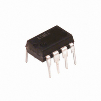
AT25040A-10PI-1.8 Atmel, AT25040A-10PI-1.8 Datasheet - Page 9

AT25040A-10PI-1.8
Manufacturer Part Number
AT25040A-10PI-1.8
Description
IC EEPROM 4KBIT 20MHZ 8DIP
Manufacturer
Atmel
Datasheet
1.AT25020AY1-10YU-1.8.pdf
(22 pages)
Specifications of AT25040A-10PI-1.8
Format - Memory
EEPROMs - Serial
Memory Type
EEPROM
Memory Size
4K (512 x 8)
Speed
5MHz, 10MHz, 20MHz
Interface
SPI, 3-Wire Serial
Voltage - Supply
1.8 V ~ 5.5 V
Operating Temperature
-40°C ~ 85°C
Package / Case
8-DIP (0.300", 7.62mm)
Lead Free Status / RoHS Status
Contains lead / RoHS non-compliant
Other names
AT25040-10PI-1.8
AT25040-10PI-1.8
AT25040-10PI-1.8
3348J–SEEPR–8/06
the data within any selected segment will therefore be read only. The block write protec-
tion levels and corresponding status register control bits are shown in Table 8.
Bits BP1 and BP0 are nonvolatile cells that have the same properties and functions as
the regular memory cells (e.g., WREN, t
Table 8. Block Write Protect Bits
READ SEQUENCE (READ): Reading the AT25010A/020A/040A via the SO pin
requires the following sequence. After the CS line is pulled low to select a device, the
read op-code (including A8) is transmitted via the SI line followed by the byte address to
be read (A7A0). Upon completion, any data on the SI line will be ignored. The data
(D7D0) at the specified address is then shifted out onto the SO line. If only one byte is
to be read, the CS line should be driven high after the data comes out. The read
sequence can be continued since the byte address is automatically incremented and
data will continue to be shifted out. When the highest address is reached, the address
counter will roll over to the lowest address allowing the entire memory to be read in one
continuous read cycle.
WRITE SEQUENCE (WRITE): In order to program the AT25010A/020A/040A, the Write
Protect pin (WP) must be held high and two separate instructions must be executed.
First, the device must be write enabled via the WREN instruction. Then a Write (WRITE)
instruction may be executed. Also, the address of the memory location(s) to be pro-
grammed must be outside the protected address field location selected by the block
write protection level. During an internal write cycle, all commands will be ignored
except the RDSR instruction.
A Write instruction requires the following sequence. After the CS line is pulled low to
select the device, the WRITE op-code (including A8) is transmitted via the SI line fol-
lowed by the byte address (A7A0) and the data (D7D0) to be programmed.
Programming will start after the CS pin is brought high. The low-to-high transition of the
CS pin must occur during the SCK low time immediately after clocking in the D0 (LSB)
data bit.
The ready/busy status of the device can be determined by initiating a Read Status Reg-
ister (RDSR) instruction. If Bit 0 = “1”, the write cycle is still in progress. If Bit 0 = “0”, the
write cycle has ended. Only the RDSR instruction is enabled during the write program-
ming cycle.
The AT25010A/020A/040A is capable of an 8-byte page write operation. After each byte
of data is received, the three low-order address bits are internally incremented by one;
the six high-order bits of the address will remain constant. If more than 8 bytes of data
are transmitted, the address counter will roll over and the previously written data will be
overwritten. The AT25010A/020A/040A is automatically returned to the write disable
state at the completion of a write cycle.
NOTE: If the WP pin is brought low or if the device is not write enabled (WREN), the
device will ignore the Write instruction and will return to the standby state, when CS is
brought high. A new CS falling edge is required to reinitiate the serial communication.
Level
1 (1/4)
2 (1/2)
3 (All)
0
Status Register Bits
BP1
0
0
1
1
BP0
0
1
0
1
WC
AT25010A
, RDSR).
607F
407F
007F
None
AT25010A/020A/040A
Array Addresses Protected
AT25020A
C0FF
80FF
00FF
None
AT25040A
180FF
1001FF
0001FF
None
9


