AT27BV512-12RI Atmel, AT27BV512-12RI Datasheet - Page 3
AT27BV512-12RI
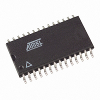
Manufacturer Part Number
AT27BV512-12RI
Description
IC OTP 512KBIT 120NS 28SOIC
Manufacturer
Atmel
Datasheet
1.AT27BV512-90JC.pdf
(12 pages)
Specifications of AT27BV512-12RI
Format - Memory
EPROMs
Memory Type
OTP EPROM
Memory Size
512K (64K x 8)
Speed
120ns
Interface
Parallel
Voltage - Supply
2.7 V ~ 3.6 V, 4.5 V ~ 5.5 V
Operating Temperature
-40°C ~ 85°C
Package / Case
28-SOIC (8.69mm width)
Lead Free Status / RoHS Status
Contains lead / RoHS non-compliant
Other names
AT27BV51212RI


Absolute Maximum Ratings*
Note:
Operating Modes
Notes:
Temperature Under Bias .................................. -40°C to +85°C
Storage Temperature ..................................... -65°C to +125°C
Voltage on Any Pin with
Respect to Ground .........................................-2.0V to +7.0V
Voltage on A9 with
Respect to Ground ......................................-2.0V to +14.0V
V
Respect to Ground .......................................-2.0V to +14.0V
Mode \ Pin
Read
Output Disable
Standby
Rapid Program
PGM Verify
PGM Inhibit
Product Identification
PP
Supply Voltage with
(2)
1.
1. X can be V
2. Read, output disable, and standby modes require, 2.7V
3. Refer to Programming Characteristics. Programming modes require V
4. V
5. Two identifier bytes may be selected. All Ai inputs are held low (V
(2)
(V
(3)
(3)
Minimum voltage is -0.6V dc which may undershoot to -2.0V for pulses of less than 20 ns. Maximum output pin voltage is
V
overshoot to +7.0V for pulses of less than 20 ns.
H
IL
CC
= 12.0
) to select the Manufacturer’s Identification byte and high (V
(2)
(3)
+ 0.75V dc which may be exceeded if certain precautions are observed (consult application notes) and which may
(3)(5)
IL
0.5V.
or V
IH
.
CE
V
V
V
V
V
V
V
IH
IH
IL
IL
IL
IL
IL
OE/V
V
V
V
(1)
(1)
(1)
V
V
V
X
PP
PP
IH
IL
IL
IL
PP
V
*NOTICE:
CC
IH
A0 = V
A1 - A15 = V
3.6V, or 4.5V
IL
) to select the Device Code byte.
), except A9 which is set to V
A9 = V
Ai
X
CC
Ai
Ai
Ai
X
X
IH
(1)
Stresses beyond those listed under “Absolute
Maximum Ratings” may cause permanent dam-
age to the device. This is a stress rating only and
functional operation of the device at these or any
other conditions beyond those indicated in the
operational sections of this specification is not
implied. Exposure to absolute maximum rating
conditions for extended periods may affect
device reliability
or V
= 6.5V.
H
(4)
IL
IL
V
CC
5.5V.
V
V
V
V
V
V
V
V
CC
CC
CC
CC
CC
CC
CC
CC
(2)
(2)
(2)
(3)
(3)
(3)
(3)
H
and A0 which is toggled low
Outputs
D
High Z
High Z
D
D
High Z
Identification Code
OUT
IN
OUT
3
Related parts for AT27BV512-12RI
Image
Part Number
Description
Manufacturer
Datasheet
Request
R

Part Number:
Description:
IC OTP 512KBIT 150NS 32PLCC
Manufacturer:
Atmel
Datasheet:

Part Number:
Description:
IC OTP 512KBIT 70NS 28SOIC
Manufacturer:
Atmel
Datasheet:
Part Number:
Description:
IC OTP 512KBIT 90NS 32PLCC
Manufacturer:
Atmel
Datasheet:
Part Number:
Description:
IC OTP 512KBIT 120NS 32PLCC
Manufacturer:
Atmel
Datasheet:
Part Number:
Description:
IC OTP 512KBIT 120NS 32PLCC
Manufacturer:
Atmel
Datasheet:
Part Number:
Description:
IC OTP 512KBIT 120NS 28SOIC
Manufacturer:
Atmel
Datasheet:

Part Number:
Description:
IC OTP 512KBIT 120NS 28TSOP
Manufacturer:
Atmel
Datasheet:
Part Number:
Description:
IC OTP 512KBIT 120NS 28TSOP
Manufacturer:
Atmel
Datasheet:
Part Number:
Description:
IC OTP 512KBIT 150NS 32PLCC
Manufacturer:
Atmel
Datasheet:
Part Number:
Description:
IC OTP 512KBIT 150NS 28SOIC
Manufacturer:
Atmel
Datasheet:
Part Number:
Description:
IC OTP 512KBIT 150NS 28SOIC
Manufacturer:
Atmel
Datasheet:
Part Number:
Description:
IC OTP 512KBIT 150NS 28TSOP
Manufacturer:
Atmel
Datasheet:
Part Number:
Description:
IC OTP 512KBIT 150NS 28TSOP
Manufacturer:
Atmel
Datasheet:
Part Number:
Description:
IC OTP 512KBIT 70NS 32PLCC
Manufacturer:
Atmel
Datasheet:
Part Number:
Description:
IC OTP 512KBIT 70NS 32PLCC
Manufacturer:
Atmel
Datasheet: