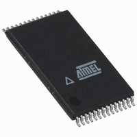
AT28BV16-30TC Atmel, AT28BV16-30TC Datasheet - Page 3

AT28BV16-30TC
Manufacturer Part Number
AT28BV16-30TC
Description
IC EEPROM 16KBIT 300NS 28TSOP
Manufacturer
Atmel
Datasheet
1.AT28BV16-25JC.pdf
(12 pages)
Specifications of AT28BV16-30TC
Format - Memory
EEPROMs - Parallel
Memory Type
EEPROM
Memory Size
16K (2K x 8)
Speed
300ns
Interface
Parallel
Voltage - Supply
2.7 V ~ 3.6 V
Operating Temperature
0°C ~ 70°C
Package / Case
28-TSOP
Lead Free Status / RoHS Status
Contains lead / RoHS non-compliant
Other names
AT28BV1630TC
Device Operation
READ: The AT28BV16 is accessed like a Static RAM.
When CE and OE are low and WE is high, the data stored
at the memory location determined by the address pins is
asserted on the outputs. The outputs are put in a high
impedance state whenever CE or OE is high. This dual line
control gives designers increased flexibility in preventing
bus contention.
BYTE WRITE: Writing data into the AT28BV16 is similar
to writing into a Static RAM. A low pulse on the WE or CE
input with OE high and CE or WE low (respectively) ini-
tiates a byte write. The address location is latched on the
last falling edge of WE (or CE); the new data is latched on
the first rising edge. Internally, the device performs a self-
clear before write. Once a byte write has been started, it
will automatically time itself to completion. Once a pro-
gramming operation has been initiated and for the duration
of t
tion.
DATA POLLING: The AT28BV16 provides DATA POLL-
ING to signal the completion of a write cycle. During a write
cycle, an attempted read of the data being written results in
WC
, a read operation will effectively be a polling opera-
the complement of that data for I/O
indeterminate). When the write cycle is finished, true data
appears on all outputs.
READY/BUSY (TSOP only): READY/BUSY is an open
drain output; it is pulled low during the internal write cycle
and released at the completion of the write cycle.
WRITE PROTECTION: Inadvertent writes to the device
are protected against in the following ways: (a) V
sense—if V
inhibited; (b) V
2.0V the device will automatically time out 5 ms (typical)
before allowing a byte write; and (c) Write Inhibit—holding
any one of OE low, CE high or WE high inhibits byte write
cycles.
DEVICE IDENTIFICATIO N:
EEPROM memory are available to the user for device iden-
tification. By raising A9 to 12
locations 7E0H to 7FFH the additional bytes may be written
to or read from in the same manner as the regular memory
array.
CC
is below 2.0V (typical) the write function is
CC
power on delay—once V
0.5V and using address
An extra 32-bytes of
7
(the other outputs are
CC
has reached
C C
3


