AT45DB161B-TI-2.5 Atmel, AT45DB161B-TI-2.5 Datasheet - Page 5
AT45DB161B-TI-2.5
Manufacturer Part Number
AT45DB161B-TI-2.5
Description
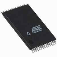
IC FLASH 16MBIT 20MHZ 28TSOP
Manufacturer
Atmel
Datasheet
1.AT45DB161B-CC.pdf
(33 pages)
Specifications of AT45DB161B-TI-2.5
Format - Memory
FLASH
Memory Type
DataFLASH
Memory Size
16M (4096 pages x 528 bytes)
Speed
20MHz
Interface
SPI, 3-Wire Serial
Voltage - Supply
2.5 V ~ 3.6 V
Operating Temperature
-40°C ~ 85°C
Package / Case
28-TSOP
Lead Free Status / RoHS Status
Contains lead / RoHS non-compliant
Available stocks
Company
Part Number
Manufacturer
Quantity
Price
Company:

Part Number:
AT45DB161B-TI-2.5
Manufacturer:
ATMEL
Quantity:
810


Program and Erase
Commands
2224I–DFLSH–10/04
loaded into the device. After the last bit of the opcode is shifted in, the eight bits of the
status register, starting with the MSB (bit 7), will be shifted out on the SO pin during the
next eight clock cycles. The five most significant bits of the status register will contain
device information, while the remaining three least-significant bits are reserved for future
use and will have undefined values. After bit 0 of the status register has been shifted
out, the sequence will repeat itself (as long as CS remains low and SCK is being tog-
gled) starting again with bit 7. The data in the status register is constantly updated, so
each repeating sequence will output new data.
Status Register Format
Ready/Busy status is indicated using bit 7 of the status register. If bit 7 is a 1, then the
device is not busy and is ready to accept the next command. If bit 7 is a 0, then the
device is in a busy state. The user can continuously poll bit 7 of the status register by
stopping SCK at a low level once bit 7 has been output. The status of bit 7 will continue
to be output on the SO pin, and once the device is no longer busy, the state of SO will
change from 0 to 1. There are eight operations which can cause the device to be in a
busy state: Main Memory Page to Buffer Transfer, Main Memory Page to Buffer Com-
pare, Buffer to Main Memory Page Program with Built-in Erase, Buffer to Main Memory
Page Program without Built-in Erase, Page Erase, Block Erase, Main Memory Page
Program, and Auto Page Rewrite.
The result of the most recent Main Memory Page to Buffer Compare operation is indi-
cated using bit 6 of the status register. If bit 6 is a 0, then the data in the main memory
page matches the data in the buffer. If bit 6 is a 1, then at least one bit of the data in the
main memory page does not match the data in the buffer.
The device density is indicated using bits 5, 4, 3 and 2 of the status register. For the
AT45DB161B, the four bits are 1, 0, 1 and 1. The decimal value of these four binary bits
does not equate to the device density; the four bits represent a combinational code
relating to differing densities of Serial DataFlash devices, allowing a total of sixteen dif-
ferent density configurations.
BUFFER WRITE: Data can be shifted in from the SI pin into either buffer 1 or buffer 2.
To load data into either buffer, an 8-bit opcode, 84H for buffer 1 or 87H for buffer 2, must
be followed by 14 don’t care bits and ten address bits (BFA9 - BFA0). The ten address
bits specify the first byte in the buffer to be written. The data is entered following the
address bits. If the end of the data buffer is reached, the device will wrap around back to
the beginning of the buffer. Data will continue to be loaded into the buffer until a low-to-
high transition is detected on the CS pin.
BUFFER TO MAIN MEMORY PAGE PROGRAM WITH BUILT-IN ERASE: Data written
into either buffer 1 or buffer 2 can be programmed into the main memory. To start the
operation, an 8-bit opcode, 83H for buffer 1 or 86H for buffer 2, must be followed by the
two reserved bits, 12 address bits (PA11 - PA0) that specify the page in the main
memory to be written, and ten additional don’t care bits. When a low-to-high transition
occurs on the CS pin, the part will first erase the selected page in main memory to all 1s
and then program the data stored in the buffer into the specified page in the main mem-
ory. Both the erase and the programming of the page are internally self-timed and
should take place in a maximum time of t
cate that the part is busy.
RDY/BUSY
Bit 7
COMP
Bit 6
Bit 5
1
Bit 4
EP
0
. During this time, the status register will indi-
Bit 3
1
Bit 2
AT45DB161B
1
Bit 1
X
Bit 0
X
5
Related parts for AT45DB161B-TI-2.5
Image
Part Number
Description
Manufacturer
Datasheet
Request
R

Part Number:
Description:
At45db161b 16-megabit 2.5-volt Only Or 2.7-volt Only Dataflash
Manufacturer:
ATMEL Corporation
Datasheet:

Part Number:
Description:
IC FLASH 16MBIT 20MHZ 24CBGA
Manufacturer:
Atmel
Datasheet:

Part Number:
Description:
IC FLASH 16MBIT 20MHZ 28TSOP
Manufacturer:
Atmel
Datasheet:

Part Number:
Description:
IC FLASH 16MBIT 20MHZ 8CASON
Manufacturer:
Atmel
Datasheet:
Part Number:
Description:
IC FLASH 16MBIT 20MHZ 8CASON
Manufacturer:
Atmel
Datasheet:

Part Number:
Description:
IC FLASH 16MBIT 20MHZ 8CASON
Manufacturer:
Atmel
Datasheet:

Part Number:
Description:
16 MEGABIT 2.5-VOLT ONLY OR 2.7-VOLT ONLY DATAFLASH
Manufacturer:
ATMEL [ATMEL Corporation]
Datasheet:
Part Number:
Description:
IC FLASH 16MBIT 20MHZ 24CBGA
Manufacturer:
Atmel
Datasheet:
Part Number:
Description:
IC FLASH 16MBIT 20MHZ 24CBGA
Manufacturer:
Atmel
Datasheet: