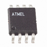
AT25256AW-10SU-1.8 Atmel, AT25256AW-10SU-1.8 Datasheet - Page 11

AT25256AW-10SU-1.8
Manufacturer Part Number
AT25256AW-10SU-1.8
Description
IC EEPROM 256KBIT 20MHZ 8SOIC
Manufacturer
Atmel
Datasheet
1.AT25128A-10PI-1.8.pdf
(24 pages)
Specifications of AT25256AW-10SU-1.8
Format - Memory
EEPROMs - Serial
Memory Type
EEPROM
Memory Size
256K (32K x 8)
Speed
5MHz, 10MHz, 20MHz
Interface
SPI, 3-Wire Serial
Voltage - Supply
1.8 V ~ 5.5 V
Operating Temperature
-40°C ~ 85°C
Package / Case
8-SOIC (5.3mm Width), 8-SOP, 8-SOEIAJ
Lead Free Status / RoHS Status
Lead free / RoHS Compliant
Other names
AT25256AW-10SU1.8
Available stocks
Company
Part Number
Manufacturer
Quantity
Price
Part Number:
AT25256AW-10SU-1.8
Manufacturer:
ATMEL/爱特梅尔
Quantity:
20 000
3368J–SEEPR–06/07
reached, the address counter will roll over to the lowest address allowing the entire memory to
be read in one continuous read cycle.
WRITE SEQUENCE (WRITE): In order to program the AT25128A/256A, two separate instruc-
tions must be executed. First, the device must be write enabled via the Write Enable (WREN)
Instruction. Then a Write instruction may be executed. Also, the address of the memory loca-
tion(s) to be programmed must be outside the protected address field location selected by the
Block Write Protection Level. During an internal write cycle, all commands will be ignored except
the RDSR instruction.
A Write Instruction requires the following sequence. After the CS line is pulled low to select the
device, the Write op-code is transmitted via the SI line followed by the byte address and the data
(D7 - D0) to be programmed (see
high. (The Low-to-High transition of the CS pin must occur during the SCK low time immediately
after clocking in the D0 (LSB) data bit.
The Ready/Busy status of the device can be determined by initiating a Read Status Register
(RDSR) Instruction. If Bit 0 = 1, the Write cycle is still in progress. If Bit 0 = 0, the Write cycle has
ended. Only the Read Status Register instruction is enabled during the Write programming
cycle.
The AT25128A/256A is capable of a 64-byte Page Write operation. After each byte of data is
received, the six low order address bits are internally incremented by one; the high order bits of
the address will remain constant. If more than 64 bytes of data are transmitted, the address
counter will roll over and the previously written data will be overwritten. The AT25128A/256A is
automatically returned to the write disable state at the completion of a Write cycle.
NOTE: If the device is not write enabled (WREN), the device will ignore the Write instruction
and will return to the standby state, when CS is brought high. A new CS falling edge is required
to re-initiate the serial communication.
Table 3-6.
Don’t Care Bits
Address
Address Key
A
N
Table
3-6). Programming will start after the CS pin is brought
AT25128A
A
A
15
13
A
A
14
0
AT25128A_256A
AT25256A
A
14
A
A
15
0
11


