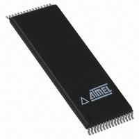
AT49F040A-70TU SL383 Atmel, AT49F040A-70TU SL383 Datasheet - Page 4

AT49F040A-70TU SL383
Manufacturer Part Number
AT49F040A-70TU SL383
Description
IC FLASH 4MBIT 70NS 32TSOP
Manufacturer
Atmel
Datasheet
1.AT49F040A-55JI.pdf
(17 pages)
Specifications of AT49F040A-70TU SL383
Format - Memory
FLASH
Memory Type
FLASH
Memory Size
4M (512K x 8)
Speed
70ns
Interface
Parallel
Voltage - Supply
4.5 V ~ 5.5 V
Operating Temperature
-40°C ~ 85°C
Package / Case
32-TSOP
Lead Free Status / RoHS Status
Lead free / RoHS Compliant
4.2
4.3
4.3.1
4.3.2
5. Byte Programming
4
Command Sequences
Erasure
AT49F040A
Chip Erase
Sector Erase
When the device is first powered on, it will be reset to the read or standby mode depending upon
the state of the control line inputs. In order to perform other device functions, a series of com-
mand sequences are entered into the device. The command sequences are shown in the
“Command Definition Table” on page
pulse on the WE or CE input with CE or WE low (respectively) and OE high. The address is
latched on the falling edge of CE or WE (except for the sixth cycle of the Sector Erase com-
mand), whichever occurs last. The data is latched by the first rising edge of CE or WE. Standard
microprocessor write timings are used. The address locations used in the command sequences
are not affected by entering the command sequences.
Before a byte can be reprogrammed, the main memory block or parameter block which contains
the byte must be erased. The erased state of the memory bits is a logical “1”. The entire device
can be erased at one time by using a 6-byte software code. The software chip erase code con-
sists of 6-byte load commands to specific address locations with a specific data pattern (please
refer to the Chip Erase Cycle Waveforms).
After the software chip erase has been initiated, the device will internally time the erase opera-
tion so that no external clocks are required. The maximum time needed to erase the whole chip
is t
erased.
If the boot block lockout has been enabled, the Chip Erase function will erase Parameter Block
1, Parameter Block 2, Main Memory Block 1 - 8 but not the boot block. If the Boot Block Lockout
has not been enabled, the Chip Erase function will erase the entire chip. After the full chip erase
the device will return back to read mode. Any command during chip erase will be ignored.
As an alternative to a full chip erase, the device is organized into sectors that can be individually
erased. There are two 8K-byte parameter block sections and eight main memory blocks. The
8K-byte parameter block sections and the eight main memory blocks can be independently
erased and reprogrammed. The Sector Erase command is a six bus cycle operation. The sector
address is latched on the rising WE edge of the sixth cycle and the 30H data input command is
also latched at the rising edge of WE. The sector erase starts after the rising edge of WE of the
sixth cycle. The erase operation is internally controlled; it will automatically time to completion.
Once the memory array is erased, the device is programmed (to a logical “0”) on a byte-by-byte
basis. Please note that a data “0” cannot be programmed back to a “1”; only erase operations
can convert “0”s to “1”s. Programming is accomplished via the internal device command register
and is a 4 bus cycle operation (please refer to the
device will automatically generate the required internal program pulses.
The program cycle has addresses latched on the falling edge of WE or CE, whichever occurs
last, and the data latched on the rising edge of WE or CE, whichever occurs first. Programming
is completed after the specified t
indicate the end of a program cycle.
EC
. If the boot block lockout feature has been enabled, the data in the boot sector will not be
BP
cycle time. The DATA polling feature may also be used to
6. The command sequences are written by applying a low
“Command Definition Table” on page
3359D–FLASH–3/05
6). The


