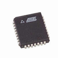
AT49LH004-33JX SL383 Atmel, AT49LH004-33JX SL383 Datasheet - Page 6

AT49LH004-33JX SL383
Manufacturer Part Number
AT49LH004-33JX SL383
Description
IC FLASH 4MBIT 33MHZ 32PLCC
Manufacturer
Atmel
Datasheet
1.AT49LH004-33JC.pdf
(40 pages)
Specifications of AT49LH004-33JX SL383
Format - Memory
FLASH
Memory Type
FLASH
Memory Size
4M (512K x 8)
Speed
33MHz
Interface
Parallel
Voltage - Supply
3 V ~ 3.6 V
Operating Temperature
0°C ~ 85°C
Package / Case
32-PLCC
Lead Free Status / RoHS Status
Lead free / RoHS Compliant
Table 5-1.
6. Interface Selection
7. FWH/LPC Interface
6
Symbol
RDY/BSY
VCC
GND
NC
RES
AT49LH004
Name and Function
READY/BUSY: The RDY/BSY pin provides the device’s ready/busy status when
using the A/A Mux interface. The RDY/BSY pin is a reflection of Status Register
bit 7, which is used to indicate whether a program or erase operation has been
completed.
Use of the RDY/BSY pin is optional, and the pin does not need to be connected.
DEVICE POWER SUPPLY: The VCC pin is used to supply the source voltage to
the device. Program and erase operations are inhibited when V
equal to V
Operations at invalid V
attempted.
GROUND: The ground reference for the power supply. GND should be connected
to the system ground.
NO CONNECT: NC pins have no internal connections and can be driven or left
floating. If the pins are driven, the voltage levels should comply with V
requirements.
RESERVED: RES pins are reserved for future device enhancements or
functionality. These pins may be left floating or may be driven. If the pins are driven,
the voltage levels should comply with V
These pins are used as the RDY/BSY and I/O[7:4] pins in the A/A Mux interface.
Signal Descriptions (Continued)
LKO
.
The AT49LH004 can operate in two distinct interface modes: The FWH/LPC interface and the
A/A Mux interface. Selection of the interface is determined by the state of the IC pin. When the
IC pin is held low, the device will operate using the FWH/LPC interface. Alternatively, when
the IC pin is held high, the device will operate using the A/A Mux interface.
The FWH/LPC interface is designed as an In-System interface used in communicating with
either the I/O Controller Hub (ICH) in Intel chipsets or typically the PCI south bridge in non-
Intel chipsets.
The FWH/LPC interface uses a 5-signal communication interface consisting of a 4-bit data
bus, the FWH/LAD[3:0] pins, and one control line, the FWH4/LFRAME pin. The operation and
timing of the interface is based on the 33 MHz PCI clock, and the buffers for the FWH/LPC
interface are PCI compliant. To ensure the effective delivery of security and manageability fea-
tures, the FWH/LPC interface is the only way to get access to the full feature set of the device.
Commands, addresses, and data are transferred via the FWH/LPC interface using a series of
fields. The field sequences and contents are strictly defined for FWH and LPC memory cycles.
These field sequences are detailed in the FWH Interface Operation and LPC Interface Opera-
tion sections.
CC
voltages may produce spurious results and should not be
IH
and V
IL
requirements.
CC
is less than or
IH
and V
IL
FWH/LPC
X
X
X
X
Interface
A/A Mux
X
X
X
X
X
3383D–FLASH–6/05
Output
Power
Power
Type
–
–


