AT45DB321C-TC Atmel, AT45DB321C-TC Datasheet - Page 2
AT45DB321C-TC
Manufacturer Part Number
AT45DB321C-TC
Description
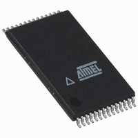
IC FLASH 32MBIT 40MHZ 28TSOP
Manufacturer
Atmel
Datasheet
1.AT45DB321C-RU.pdf
(40 pages)
Specifications of AT45DB321C-TC
Format - Memory
FLASH
Memory Type
DataFLASH
Memory Size
32M (8192 pages x 528 bytes)
Speed
40MHz
Interface
SPI, 3-Wire Serial
Voltage - Supply
2.7 V ~ 3.6 V
Operating Temperature
0°C ~ 70°C
Package / Case
28-TSOP
Lead Free Status / RoHS Status
Contains lead / RoHS non-compliant


2. Pin Configurations and Packages
Table 2-1.
2
RDY/BUSY
Pin Name
CS
SCK
SI
SO
WP
RESET
RDY/BUSY
Figure 2-1.
Figure 2-4.
Note:
RESET
GND
VCC
SCK
WP
NC
NC
NC
NC
NC
SO
CS
SI
1. See AT45DCB004C Datasheet
1
2
3
4
5
6
7
8
9
10
11
12
13
14
AT45DB321C
Pin Configurations
TSOP Top View – Type 1
DataFlash Card
through Package
7 6
5 4 3 2 1
To allow for simple in-system reprogrammability, the AT45DB321C does not require high input
voltages for programming. The device operates from a single power supply, 2.7V to 3.6V, for
both the program and read operations. The AT45DB321C is enabled through the chip select pin
(CS) and accessed via a three-wire interface consisting of the Serial Input (SI), Serial Output
(SO), and the Serial Clock (SCK).
All programming and erase cycles are self-timed.
(1)
Top View
28
27
26
25
24
23
22
21
20
19
18
17
16
15
NC
NC
NC
NC
NC
NC
NC
NC
NC
NC
NC
NC
NC
NC
Function
Chip Select
Serial Clock
Serial Input
Serial Output
Hardware Page Write Protect Pin
Chip Reset
Ready/Busy
Figure 2-2.
Figure 2-5.
RESET
A
B
C
D
E
SCK
CS
SI
NC
NC
NC
NC
1
1
2
3
4
SCK
NC
CS
SO
NC
CBGA Top View
through Package
2
CASON – Top View
through Package
RDY/BSY
GND
NC
NC
3
SI
RESET
VCC
WP
NC
NC
4
8
7
6
5
NC
NC
NC
NC
NC
5
SO
GND
VCC
WP
Figure 2-3.
GND
SCK
NC
NC
SO
NC
NC
NC
NC
NC
NC
NC
CS
SI
1
2
3
4
5
6
7
8
9
10
11
12
13
14
SOIC Top View
28
27
26
25
24
23
22
21
20
19
18
17
16
15
3387M–DFLASH–2/08
VCC
NC
NC
WP
RESET
RDY/BUSY
NC
NC
NC
NC
NC
NC
NC
NC
Related parts for AT45DB321C-TC
Image
Part Number
Description
Manufacturer
Datasheet
Request
R

Part Number:
Description:
DEV KIT FOR AVR/AVR32
Manufacturer:
Atmel
Datasheet:

Part Number:
Description:
INTERVAL AND WIPE/WASH WIPER CONTROL IC WITH DELAY
Manufacturer:
ATMEL Corporation
Datasheet:
Part Number:
Description:
Low-Voltage Voice-Switched IC for Hands-Free Operation
Manufacturer:
ATMEL Corporation
Datasheet:
Part Number:
Description:
MONOLITHIC INTEGRATED FEATUREPHONE CIRCUIT
Manufacturer:
ATMEL Corporation
Datasheet:
Part Number:
Description:
AM-FM Receiver IC U4255BM-M
Manufacturer:
ATMEL Corporation
Datasheet:
Part Number:
Description:
Monolithic Integrated Feature Phone Circuit
Manufacturer:
ATMEL Corporation
Datasheet:
Part Number:
Description:
Multistandard Video-IF and Quasi Parallel Sound Processing
Manufacturer:
ATMEL Corporation
Datasheet:
Part Number:
Description:
High-performance EE PLD
Manufacturer:
ATMEL Corporation
Datasheet:
Part Number:
Description:
8-bit Flash Microcontroller
Manufacturer:
ATMEL Corporation
Datasheet:
Part Number:
Description:
2-Wire Serial EEPROM
Manufacturer:
ATMEL Corporation
Datasheet: