CY7C185-15VC Cypress Semiconductor Corp, CY7C185-15VC Datasheet

IC SRAM 64KBIT 15NS 28SOJ

CY7C185-15VC

Manufacturer Part Number
CY7C185-15VC
Description
IC SRAM 64KBIT 15NS 28SOJ
Manufacturer
Cypress Semiconductor Corp
Datasheet

Specifications of CY7C185-15VC

Format - Memory
RAM
Memory Type
SRAM - Asynchronous
Memory Size
64K (8K x 8)
Speed
15ns
Interface
Parallel
Voltage - Supply
4.5 V ~ 5.5 V
Operating Temperature
0°C ~ 70°C
Package / Case
28-SOJ
Lead Free Status / RoHS Status
Contains lead / RoHS non-compliant
Other names
428-1052

Available stocks

Company
Part Number
Manufacturer
Quantity
Price
Part Number:
CY7C185-15VC
Manufacturer:
CYPRESS
Quantity:
6 100
Part Number:
CY7C185-15VC
Manufacturer:
CY
Quantity:
1
Part Number:
CY7C185-15VC
Manufacturer:
TOSHIBA
Quantity:
2 988
Part Number:
CY7C185-15VC
Manufacturer:
HAR
Quantity:
15
Part Number:
CY7C185-15VC
Quantity:
200
Part Number:
CY7C185-15VC
Manufacturer:
CYPRESS/赛普拉斯
Quantity:
20 000
Part Number:
CY7C185-15VCT
Quantity:
200
Part Number:
CY7C185-15VCT
Manufacturer:
CYPRESS/赛普拉斯
Quantity:
20 000
Cypress Semiconductor Corporation
Document #: 38-05043 Rev. *A
Features
Functional Description
The CY7C185 is a high-performance CMOS static RAM orga-
nized as 8192 words by 8 bits. Easy memory expansion is
Selection Guide
Maximum Access Time (ns)
Maximum Operating Current (mA)
Maximum Standby Current (mA)
Note:
• High speed
• Fast t
• Low active power
• Low standby power
• CMOS for optimum speed/power
• Easy memory expansion with CE
• TTL-compatible inputs and outputs
• Automatic power-down when deselected
1.
2.
Logic Block Diagram
— 15 ns
— 715 mW
— 220 mW
For guidelines on SRAM system design, please refer to the ‘System Design Guidelines’ Cypress application note, available on the internet at www.cypress.com.
For military specifications, see the CY7C185A data sheet.
CE
CE
WE
OE
1
2
DOE
A
A
A
A
A
A
A
A
1
2
3
4
5
6
7
8
[2]
COLUMN DECODER
[1]
INPUT BUFFER
256 x 32 x 8
ARRAY
1
, CE
2
, and OE features
3901 North First Street
POWER
DOWN
7C185-15
40/15
130
15
provided by an active LOW chip enable (CE
chip enable (CE
three-state drivers. This device has an automatic power-down
feature (CE
when deselected. The CY7C185 is in a standard 300-mil-wide
DIP, SOJ, or SOIC package.
An active LOW write enable signal (WE) controls the writ-
ing/reading operation of the memory. When CE
puts are both LOW and CE
input/output pins (I/O
location addressed by the address present on the address
pins (A
selecting the device and enabling the outputs, CE
active LOW, CE
HIGH. Under these conditions, the contents of the location ad-
dressed by the information on address pins are present on the
eight data input/output pins.
The input/output pins remain in a high-impedance state unless
the chip is selected, outputs are enabled, and write enable
(WE) is HIGH. A die coat is used to insure alpha immunity.
7C185-20
0
20/15
through A
110
20
I/O
I/O
I/O
I/O
I/O
I/O
I/O
I/O
1
San Jose
or CE
0
1
2
3
4
5
6
7
2
2
), and active LOW output enable (OE) and
active HIGH, while WE remains inactive or
12
2
), reducing the power consumption by 70%
). Reading the device is accomplished by
0
through I/O
8K x 8 Static RAM
7C185-25
2
20/15
CA 95134
100
is HIGH, data on the eight data
25
Pin Configurations
GND
Revised September 13, 2002
I/O
I/O
I/O
A
A
A
NC
A
A
A
A
A
A
10
11
12
7
4
5
6
7
8
9
0
1
2
) is written into the memory
DIP/SOJ/SOIC
Top View
1
2
3
4
5
6
7
8
9
10
11
12
13
14
1
28
27
26
25
24
23
22
21
20
19
18
17
16
15
), an active HIGH
CY7C185
7C185-35
408-943-2600
1
V
WE
CE
A
A
A
OE
A
CE
I/O
I/O
I/O
I/O
I/O
20/15
CC
3
2
1
0
100
and WE in-
7
6
5
4
3
2
1
35
1
and OE

Related parts for CY7C185-15VC

CY7C185-15VC Summary of contents

Page 1

... CMOS for optimum speed/power • Easy memory expansion with CE • TTL-compatible inputs and outputs • Automatic power-down when deselected [1] Functional Description The CY7C185 is a high-performance CMOS static RAM orga- nized as 8192 words by 8 bits. Easy memory expansion is Logic Block Diagram INPUT BUFFER A 1 ...

Page 2

... CC Output Disabled V = Max GND OUT V = Max OUT Max Min. Duty Cycle = 100% Max – 0.3V 0. – CY7C185 Ambient Temperature + 10% – + 10% 7C185-15 7C185-20 Min. Max. Min. Max. Unit 2.4 2.4 V 0.4 0 0.3V 0.3V –0.5 0.8 –0.5 0.8 V –5 +5 –5 +5 – ...

Page 3

... Min. Duty Cycle = 100% Max – – Test Conditions MHz 5. 481 255 INCLUDING JIGAND SCOPE (b) 1.73V CY7C185 7C185-25 7C185-35 Min. Max. Min. Max. 2.4 2.4 0.4 0 0.3V 0.3V –0.5 0.8 –0.5 0.8 –5 +5 –5 +5 –5 +5 –5 +5 –300 –300 100 ...

Page 4

... AC Test Loads. Transition is measured 500 mV from steady state voltage less than t and t for any given device. HZCE LZCE1 LZCE2 LOW, CE HIGH, and WE LOW. All 3 signals must be active to initiate a write and either 1 2 CY7C185 7C185-25 7C185-35 Max. Min. Max. Min. Max ...

Page 5

... LOW, CE HIGH and WE LOW going HIGH or CE going LOW. The data input set-up and hold timing should be referenced to the 1 2 DATA VALID t HZOE t HZCE DATA VALID VALID and WE must be LOW and CE 1 CY7C185 HIGH IMPEDANCE ICC ISB must be HIGH 2 Page ...

Page 6

... The minimum write cycle time for write cycle #3 (WE controlled, OE LOW) is the sum goes HIGH or CE goes LOW simultaneously with WE HIGH, the output remains in a high-impedance state Document #: 38-05043 Rev SCE1 SCE2 t AW DATA [13,14,15,16 SCE1 t SCE2 t AW DATA HZWE VALID VALID IN t LZWE and t . HZWE SD CY7C185 Page ...

Page 7

... OUTPUT VOLTAGE (V) OUTPUT SINK CURRENT vs. OUTPUT VOLTAGE 140 120 100 = 125 0.0 1.0 2.0 OUTPUT VOLTAGE (V) NORMALIZED I vs. CYCLE TIME CC 1.25 V =5. = =0.5V CC 1.00 0.75 0.50 1000 CYCLE FREQUENCY (MHz) CY7C185 =5.0V =25 C 3.0 4.0 =5.0V 3.0 4.0 40 Page ...

Page 8

... Pin Name Function Number A10 Y4 A11 Y3 A12 Ordering Information Speed (ns) Ordering Code 15 CY7C185-15PC CY7C185-15SC CY7C185-15VC CY7C185-15VI 20 CY7C185-20PC CY7C185-20SC CY7C185-20VC CY7C185-20VI 25 CY7C185-25PC CY7C185-25SC CY7C185-25VC CY7C185-25VI 35 CY7C185-35PC CY7C185-35SC CY7C185-35VC CY7C185-35VI Document #: 38-05043 Rev Input/Output X High Z X High Z L Data Out X Data In H High ...

Page 9

... Package Diagrams Document #: 38-05043 Rev. *A 28-Lead (300-Mil) Molded DIP P21 28-Lead (300-Mil) Molded SOIC S21 CY7C185 51-85014-*B 51-85026-*A Page ...

Page 10

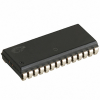
... The inclusion of Cypress Semiconductor products in life-support systems application implies that the manufacturer assumes all risk of such use and in doing so indemnifies Cypress Semiconductor against all charges. 28-Lead (300-Mil) Molded SOJ V21 CY7C185 51-85031-*B Page ...

Page 11

... Document History Page Document Title: CY7C185 Static RAM Document Number: 38-05043 Issue REV. ECN NO. Date ** 107145 09/10/01 *A 116470 09/16/02 Document #: 38-05043 Rev. *A Orig. of Change Description of Change SZV Change from Spec number: 38-00037 to 38-05043 CEA Add applications foot note to data sheet. CY7C185 ...

Related keywords