CY62148BLL-70SC Cypress Semiconductor Corp, CY62148BLL-70SC Datasheet
CY62148BLL-70SC
Specifications of CY62148BLL-70SC
Available stocks


Related parts for CY62148BLL-70SC

CY62148BLL-70SC Summary of contents
Page 1
... COLUMN CE DECODER WE OE Cypress Semiconductor Corporation Document #: 38-05039 Rev. *C 4-Mbit (512K x 8) Static RAM is provided by an active LOW Chip Enable (CE), an active LOW Output Enable (OE), and three-state drivers. This device has an automatic power-down feature that reduces power consumption by more than 99% when deselected. ...
Page 2
... Product Portfolio V CC Product Min. Typ. CY62148BLL 4.5 V 5.0V Maximum Ratings (Above which the useful life may be impaired. For user guide- lines, not tested.) Storage Temperature ................................. –65°C to +150°C Ambient Temperature with Power Applied............................................. –55°C to +125°C Supply Voltage Relative GND........ – ...
Page 3
Capacitance Parameter Description C Input Capacitance IN C Output Capacitance OUT AC Test Loads and Waveforms R1 1800 Ω 5V OUTPUT OUTPUT R2 100 pF 990 Ω INCLUDING JIG AND SCOPE (a) Note: 4. Tested initially and after any ...
Page 4
... HZWE 8. The internal write time of the memory is defined by the overlap of CE LOW, and WE LOW. CE and WE must be LOW to initiate a write, and the transition of any of these signals can terminate the write. The input data set-up and hold timing should be referenced to the leading edge of the signal that terminates the write. ...
Page 5
Data Retention Characteristics Parameter Description V V for Data Retention Data Retention Current CCDR [4] t Chip Deselect to Data Retention Time CDR [9] t Operation Recovery Time R Data Retention Waveform Switching Waveforms ...
Page 6
Switching Waveforms (continued) Write Cycle No. 1 (CE Controlled) ADDRESS CE WE DATA I/O Write Cycle No. 2 (WE Controlled, OE HIGH During Write) ADDRESS DATA I/O NOTE 15 t HZOE Notes: 13. If ...
Page 7
... WE I High Data Out Data High Z Ordering Information Speed Ordering Code (ns) 70 CY62148BLL-70SC CY62148BLL-70ZC CY62148BLL-70ZRC CY62148BLL-70SI CY62148BLL-70ZI CY62148BLL-70ZRI Please contact your local Cypress sales representative for availability of these parts Document #: 38-05039 Rev. *C [13, 14 SCE PWE t HZWE – I/O Mode 0 7 Power-Down ...
Page 8
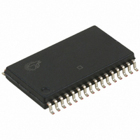
Package Diagrams Document #: 38-05039 Rev. *C 32-lead (450 MIL) Molded SOIC (51-85081) CY62148B MoBL™ 51-85081-A Page ...
Page 9
Package Diagrams (continued) 32-lead Thin Small Outline Package Type II (51-85095) All products and company names mentioned in this document may be the trademarks of their respective holders. Document #: 38-05039 Rev. *C CY62148B MoBL™ 51-85095-** Page ...
Page 10
... Document #: 38-05039 Rev. *C © Cypress Semiconductor Corporation, 2006. The information contained herein is subject to change without notice. Cypress Semiconductor Corporation assumes no responsibility for the use of any circuitry other than circuitry embodied in a Cypress product. Nor does it convey or imply any license under patent or other rights. Cypress products are not warranted nor intended to be used for medical, life support, life saving, critical control or safety applications, unless pursuant to an express written agreement with Cypress ...
Page 11
... MGN Remove 55-ns devices VKN Changed address of Cypress Semiconductor Corporation on Page# 1 from “3901 North First Street” to “198 Champion Court” Corrected the typo in the Array size in the Logic Block Diagram on page# 1 Renamed Package Name column with Package Diagram in the Ordering Information Table CY62148B MoBL™ ...