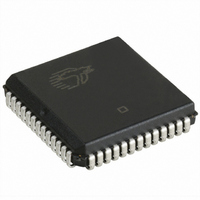
CY7C131-25JC Cypress Semiconductor Corp, CY7C131-25JC Datasheet - Page 6

CY7C131-25JC
Manufacturer Part Number
CY7C131-25JC
Description
IC SRAM 8KBIT 25NS 52PLCC
Manufacturer
Cypress Semiconductor Corp
Specifications of CY7C131-25JC
Format - Memory
RAM
Memory Type
SRAM - Dual Port, Asynchronous
Memory Size
8K (1K x 8)
Speed
25ns
Interface
Parallel
Voltage - Supply
4.5 V ~ 5.5 V
Operating Temperature
0°C ~ 70°C
Package / Case
52-PLCC
Density
8Kb
Access Time (max)
25ns
Sync/async
Asynchronous
Architecture
Not Required
Clock Freq (max)
Not RequiredMHz
Operating Supply Voltage (typ)
5V
Address Bus
10b
Package Type
PLCC
Operating Temp Range
0C to 70C
Number Of Ports
2
Supply Current
170mA
Operating Supply Voltage (min)
4.5V
Operating Supply Voltage (max)
5.5V
Operating Temperature Classification
Commercial
Mounting
Surface Mount
Pin Count
52
Word Size
8b
Number Of Words
1K
Lead Free Status / RoHS Status
Contains lead / RoHS non-compliant
Other names
428-1193
Available stocks
Company
Part Number
Manufacturer
Quantity
Price
Company:
Part Number:
CY7C131-25JC
Manufacturer:
CYP
Quantity:
5 510
Company:
Part Number:
CY7C131-25JC
Manufacturer:
Cypress Semiconductor Corp
Quantity:
10 000
Part Number:
CY7C131-25JC
Manufacturer:
CYPRESS/赛普拉斯
Quantity:
20 000
Switching Characteristics
Switching Waveforms
Notes:
19. R/W is HIGH for read cycle.
20. Device is continuously selected, CE = V
t
t
t
t
t
t
t
t
t
t
t
t
t
t
t
t
t
t
t
t
t
t
t
t
t
t
WC
SCE
AW
HA
SA
PWE
SD
HD
HZWE
LZWE
BLA
BHA
BLC
BHC
PS
WB
WH
BDD
DDD
WDD
WINS
EINS
INS
OINR
EINR
INR
WRITE CYCLE
BUSY/INTERRUPT TIMING
INTERRUPT TIMING
Parameter
Read Cycle No.1
DATA OUT
ADDRESS
[17]
Write Cycle Time
CE LOW to Write End
Address Set-Up to Write End
Address Hold from Write End
Address Set-Up to Write Start
R/W Pulse Width
Data Set-Up to Write End
Data Hold from Write End
R/W LOW to High Z
R/W HIGH to Low Z
BUSY LOW from Address Match
BUSY HIGH from Address Mismatch
BUSY LOW from CE LOW
BUSY HIGH from CE HIGH
Port Set Up for Priority
R/W LOW after BUSY LOW
R/W HIGH after BUSY HIGH
BUSY HIGH to Valid Data
Write Data Valid to Read Data Valid
Write Pulse to Data Delay
R/W to INTERRUPT Set Time
CE to INTERRUPT Set Time
Address to INTERRUPT Set Time
OE to INTERRUPT Reset Time
CE to INTERRUPT Reset Time
Address to INTERRUPT Reset Time
[15]
PREVIOUS DATA VALID
[19, 20]
t
OHA
Description
Over the Operating Range
[14]
[14]
IL
and OE = V
[16]
IL
.
[16]
[16]
[16]
Either Port Address Access
[16]
t
AA
[6,11]
t
RC
6
(continued)
Min.
35
30
30
25
15
30
2
0
0
0
5
0
7C130-35
7C131-35
7C140-35
7C141-35
Max.
Note
Note
20
20
20
20
20
35
18
18
25
25
25
25
25
25
Min.
45
35
35
30
20
35
7C130-45
7C131-45
7C140-45
7C141-45
2
0
0
0
5
0
DATA VALID
CY7C130/CY7C131
CY7C140/CY7C141
Max.
Note
Note
20
25
25
25
25
45
18
18
35
35
35
35
35
35
Min.
55
40
40
30
20
35
7C130-55
7C131-55
7C140-55
7C141-55
2
0
0
0
5
0
Max.
Note
Note
25
30
30
30
30
45
18
18
45
45
45
45
45
45
C130-7
Unit
ns
ns
ns
ns
ns
ns
ns
ns
ns
ns
ns
ns
ns
ns
ns
ns
ns
ns
ns
ns
ns
ns
ns
ns
ns
ns


