CY7C146-25JC Cypress Semiconductor Corp, CY7C146-25JC Datasheet
CY7C146-25JC
Specifications of CY7C146-25JC
Available stocks


Related parts for CY7C146-25JC


CY7C146-25JC Summary of contents
Page 1
... CC • Fully asynchronous operation • Automatic power-down • Master CY7C132/CY7C136 easily expands data bus width more bits using slave CY7C142/CY7C146 • BUSY output flag on CY7C132/CY7C136; BUSY input on CY7C142/CY7C146 • INT flag for port-to-port communication (52-pin PLCC/PQFP versions) • Available in 48-pin DIP (CY7C132/142), 52-pin PLCC and 52-pin TQFP (CY7C136/146) • ...
Page 2
... I [3] 7C132-25 7C132-30 7C136-25 7C136-30 [3] 7C136-15 7C142-25 7C142-30 7C146-15 7C146-25 7C146- 190 170 170 CY7C132/CY7C136 CY7C142/CY7C146 PQFP Top View 7C136 33 7C146 1415 7C132-35 7C132-45 7C132-55 7C136-35 7C136-45 7C136-55 7C142-35 7C142-45 7C142-55 7C146-35 7C146-45 7C146- 120 120 110 170 170 ...
Page 3
... V < Mil [8] MAX Test Conditions MHz 5.0V CC and using AC Test Waveforms input levels of GND to 3V. rc CY7C132/CY7C136 CY7C142/CY7C146 Ambient Temperature 0°C to +70°C –40°C to +85–C [4] –55°C to +125°C [3] 7C132-30 7C132-35,45 7C136-25,30 7C136-35,45 [3] 7C142-30 7C142-35,45 7C146-25,30 7C146-35,45 2.4 2.4 ...
Page 4
... HZCE LZCE are tested with C = 5pF Test Loads. Transition is measured ±500 mV from steady-state voltage. L CY7C132/CY7C136 CY7C142/CY7C146 5V 281 BUSY OR INT 30 pF BUSY Output Load (CY7C132/CY7C136 Only) ALL INPUT PULSES 90% 90% 10% < [5, 10] [3] 7C132-25 7C132-30 7C136-25 7C136-30 7C142-25 ...
Page 5
... These parameters are measured from the input signal changing, until the output pin goes to a high-impedance state. 16. CY7C142/CY7C146 only. 17. A write operation on Port A, where Port A has priority, leaves the data on Port B’s outputs undisturbed until one access time after one of the following: BUSY on Port B goes HIGH. Port B’ ...
Page 6
... CE to INTERRUPT Reset Time EINR t Address to INTERRUPT Reset Time INR Document #: 38-06031 Rev. *A 7C132-35 7C136-35 7C142-35 7C146-35 Min. Max [ [15 [15 [16 Note 17 Note [15] 25 [15] 25 [15] 25 CY7C132/CY7C136 CY7C142/CY7C146 [5, 10] 7C132-45 7C132-55 7C136-45 7C136-55 7C142-45 7C142-55 7C146-45 7C146-55 Min. Max. Min. Max ...
Page 7
... Address valid prior to or coincident with CE transition LOW. Document #: 38-06031 Rev. *A [19, 20 [19, 21] t ACE t DOE t RC ADDRESS MATCH t PWE t PS ADDRESS MATCH t BLA and CY7C132/CY7C136 CY7C142/CY7C146 DATA VALID t HZCE t HZOE DATA VALID t PD VALID t BHA t BDD t DDD t WDD VALID Page ...
Page 8
... If the CE LOW transition occurs simultaneously with or after the R/W LOW transition, the outputs remain in a high-impedance state. Document #: 38-06031 Rev. *A [14, 22 SCE PWE t SD DATA VALID HIGH IMPEDANCE [14, 23 SCE PWE t SD DATA VALID t HZWE HIGH IMPEDANCE allow the data I/O pins to enter high impedance and for data PWE HZWE SD CY7C132/CY7C136 CY7C142/CY7C146 LZWE Page ...
Page 9
... Busy Timing Diagram No. 2 (Address Arbitration) Left Address ValidFirst: ADDRESS ADDRESS MATCH ADDRESS R BUSY R RightAddressValidFirst: ADDRESS ADDRESS MATCH ADDRESS L BUSY L Document #: 38-06031 Rev. *A ADDRESS MATCH BLC ADDRESS MATCH BLC ADDRESS MISMATCH t t BLA BHA ADDRESS MISMATCH t t BLA BHA CY7C132/CY7C136 CY7C142/CY7C146 t BHC t BHC Page ...
Page 10
... Switching Waveforms (continued) Busy Timing Diagram No. 3 (Write with BUSY, Slave: CY7C142/CY7C146 BUSY [18] Interrupt Timing Diagrams Left Side Sets INT : R ADDRESS R INT R Right Side Clears INT : R ADDRESS R INT R Right Side Sets INT : L ADDRESS R INT L Document #: 38-06031 Rev PWE t WC WRITE 7FF ...
Page 11
... AMBIENTTEMPERATURE(°C) TYPICAL ACCESS TIME CHANGE vs. OUTPUT LOADING 30.0 25.0 20.0 15.0 10.0 V =4.5V CC 5.0 T =25° 5.0 0 200 400 600 800 1000 CAPACITANCE (pF) CY7C132/CY7C136 CY7C142/CY7C146 t RC READ 7FE t INR t OINR OUTPUT SOURCE CURRENT vs. OUTPUT VOLTAGE 120 100 =5. =25° 125 0 1 ...
Page 12
... Molded DIP P25 48-Lead (600-Mil) Molded DIP D26 48-Lead (600-Mil) Sidebraze DIP P25 48-Lead (600-Mil) Molded DIP P25 48-Lead (600-Mil) Molded DIP D26 48-Lead (600-Mil) Sidebraze DIP CY7C132/CY7C136 CY7C142/CY7C146 Operating Range Commercial Industrial Commercial Industrial Military Commercial Industrial Military Commercial ...
Page 13
... Ordering Information (continued) Speed (ns) Ordering Code 15 CY7C146-15JC CY7C146-15NC 25 CY7C146-25JC CY7C146-25NC 30 CY7C146-30JC CY7C146-30NC CY7C146-30JI 35 CY7C146-35JC CY7C146-35NC CY7C146-35JI CY7C146-35LMB 45 CY7C146-45JC CY7C146-45NC CY7C146-45JI CY7C146-45LMB 55 CY7C146-55JC CY7C146-55NC CY7C146-55JI CY7C146-55LMB MILITARY SPECIFICATIONS Group A Subgroup Testing—DC Characteristics Parameter Max SB1 I SB2 I SB3 I SB4 Switching Characteristics Parameter ...
Page 14
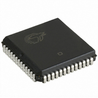
... Package Diagrams Document #: 38-06031 Rev. *A 48-Lead (600-Mil) Sidebraze DIP D26 MIL-STD-1835 D-14 Config. C 52-Lead Plastic Leaded Chip Carrier J69 CY7C132/CY7C136 CY7C142/CY7C146 51-80044-** 51-85004-*A Page ...
Page 15
... Package Diagrams (continued) Document #: 38-06031 Rev. *A 52-Square Leadless Chip Carrier L69 52-Lead Plastic Quad Flatpack N52 CY7C132/CY7C136 CY7C142/CY7C146 51-80054-** 51-85042-** Page ...
Page 16
... The inclusion of Cypress Semiconductor products in life-support systems application implies that the manufacturer assumes all risk of such use and in doing so indemnifies Cypress Semiconductor against all charges. 48-Lead (600-Mil) Molded DIP P25 CY7C132/CY7C136 CY7C142/CY7C146 51-85020-*A Page ...
Page 17
... Document History Page Document Title: CY7C132 / CY7C136 / CY7C142 / CY7C146 Dual Port Static RAM Document Number: 38-06031 REV. ECN NO. Issue Date ** 110171 10/21/01 *A 128959 9/03/03 Document #: 38-06031 Rev. *A Orig. of Change Description of Change SZV Change from Spec number: 38-06031 JFU Added CY7C136-55NI to Order Information ...