CY7C1049CV33-20VC Cypress Semiconductor Corp, CY7C1049CV33-20VC Datasheet - Page 2
CY7C1049CV33-20VC
Manufacturer Part Number
CY7C1049CV33-20VC
Description
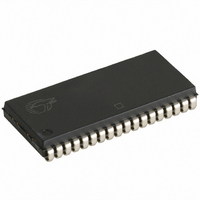
IC SRAM 4MBIT 20NS 36SOJ
Manufacturer
Cypress Semiconductor Corp
Datasheet
1.CY7C1049CV33-15VC.pdf
(7 pages)
Specifications of CY7C1049CV33-20VC
Format - Memory
RAM
Memory Type
SRAM - Asynchronous
Memory Size
4M (512K x 8)
Speed
20ns
Interface
Parallel
Voltage - Supply
3 V ~ 3.6 V
Operating Temperature
0°C ~ 70°C
Package / Case
36-SOJ
Lead Free Status / RoHS Status
Contains lead / RoHS non-compliant
Other names
428-1488-5
Available stocks
Company
Part Number
Manufacturer
Quantity
Price
Company:

Part Number:
CY7C1049CV33-20VC
Manufacturer:
CYPRESS
Quantity:
5 380


Document #: 38-05006 Rev. *B
Maximum Ratings
(Above which the useful life may be impaired. For user guide-
lines, not tested.)
Storage Temperature .................................–65 C to +150 C
Ambient Temperature with
Power Applied............................................. –55 C to +125 C
Supply Voltage on V
Electrical Characteristics
Capacitance
AC Test Loads and Waveforms
V
V
V
V
I
I
I
I
I
C
C
Notes:
IX
OZ
CC
SB1
SB2
Parame-
3.
4.
5.
OH
OL
IH
IL
IN
OUT
ter
V
Tested initially and after any design or process changes that may affect these parameters.
AC characteristics (except High-Z) for all 8-ns and 10-ns parts are tested using the load conditions shown in Figure (a). All other speeds are tested using the
Thevenin load shown in Figure (b). High-Z characteristics are tested for all speeds using the test load shown in Figure (d).
IL
Parameter
* CAPACITIVE LOAD CONSISTS
OF ALL COMPONENTS OF THE
TEST ENVIRONMENT
(min.) = –2.0V for pulse durations of less than 20 ns.
8-, 10-ns devices:
GND
3.0V
Output HIGH Voltage
Output LOW Voltage
Input HIGH Voltage
Input LOW Voltage
Input Load Current
Output Leakage
Current
V
Supply Current
Automatic CE
Power-down Current
—TTL Inputs
Automatic CE
Power-down Current
—CMOS Inputs
Rise Time: 1 V/ns
CC
OUTPUT
[4]
Operating
Description
CC
to Relative GND
Input Capacitance
I/O Capacitance
10%
90%
[3]
Z = 50
Description
Over the Operating Range
ALL INPUT PULSES
V
V
GND < V
GND < V
Output Disabled
V
f = f
Max. V
V
Max. V
CE > V
V
or V
CC
CC
CC
IN
IN
[3]
MAX
< V
> V
[5]
IN
(a)
(c)
= Min.; I
= Min.,; I
= Max.,
1.5V
50
.... –0.5V to +4.6V
< 0.3V, f = 0
CC
CC
Test Conditions
CC
IL
CC
= 1/t
, f = f
I
OUT
, CE > V
,
< V
– 0.3V,
– 0.3V,
OH
RC
OL
< V
CC
MAX
= –4.0 mA
= 8.0 mA
CC
IH
Fall Time: 1 V/ns
90%
; V
T
V
30 pF*
,
Comm’l
Ind’l
Com’l/Ind’l
A
CC
10%
IN
= 25 C, f = 1 MHz,
High-Z characteristics:
= 3.3V
> V
IH
Test Conditions
or
DC Voltage Applied to Outputs
in High-Z State
DC Input Voltage
Current into Outputs (LOW)......................................... 20 mA
Operating Range
Commercial
Industrial
Min. Max. Min. Max. Min. Max. Min. Max.
–0.3
2.4
2.0
–1
–1
Range
-8
[2]
+ 0.3
V
100
110
0.4
0.8
+1
+1
40
10
12-, 15-ns devices:
CC
OUTPUT
OUTPUT
[3]
–0.3
.................................... –0.5V to V
[3]
2.4
2.0
–1
–1
3.3V
3.3V
Ambient Temperature
................................ –0.5V to V
-10
–40 C to +85 C
+ 0.3
V
100
0 C to +70 C
0.4
0.8
+1
+1
90
40
10
30 pF
CC
5 pF
–0.3
2.4
2.0
(d)
(b)
–1
–1
Max.
8
8
R 317
-12
CY7C1049CV33
R 317
+ 0.3
V
0.4
0.8
+1
+1
85
95
40
10
CC
351
351
–0.3
2.4
2.0
R2
R2
–1
–1
3.3V
-15
Page 2 of 7
+ 0.3
V
V
Unit
0.4
0.8
CC
CC
+1
+1
80
90
40
10
pF
pF
CC
CC
0.3V
+ 0.5V
+ 0.5V
Unit
mA
mA
mA
mA
V
V
V
V
A
A
Related parts for CY7C1049CV33-20VC
Image
Part Number
Description
Manufacturer
Datasheet
Request
R

Part Number:
Description:
Manufacturer:
Cypress Semiconductor Corp
Datasheet:
Part Number:
Description:
Manufacturer:
Cypress Semiconductor Corp
Datasheet:
Part Number:
Description:
Manufacturer:
Cypress Semiconductor Corp
Datasheet:
Part Number:
Description:
Manufacturer:
Cypress Semiconductor Corp
Datasheet:
Part Number:
Description:
Manufacturer:
Cypress Semiconductor Corp
Datasheet: