PSD834F2-70J STMicroelectronics, PSD834F2-70J Datasheet - Page 57
PSD834F2-70J
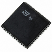
Manufacturer Part Number
PSD834F2-70J
Description
IC FLASH 2MBIT 70NS 52PLCC
Manufacturer
STMicroelectronics
Datasheet
1.PSD813F2VA-20JI.pdf
(109 pages)
Specifications of PSD834F2-70J
Format - Memory
FLASH
Memory Type
FLASH
Memory Size
2M (256K x 8)
Speed
70ns
Interface
Parallel
Voltage - Supply
4.5 V ~ 5.5 V
Operating Temperature
0°C ~ 70°C
Package / Case
52-PLCC
Lead Free Status / RoHS Status
Lead free / RoHS Compliant
Other names
497-2004-5
Available stocks
Company
Part Number
Manufacturer
Quantity
Price
Company:

Part Number:
PSD834F2-70J
Manufacturer:
WSI
Quantity:
409
Company:
Part Number:
PSD834F2-70J
Manufacturer:
STMicroelectronics
Quantity:
10 000


Table 26. Drive Register Pin Assignment
Note: 1. NA = Not Applicable.
Port Data Registers
The Port Data Registers, shown in Table 27, are
used by the MCU to write data to or read data from
the ports. Table
ports having each register type, and MCU access
for each register type. The registers are described
below.
Data In
Port pins are connected directly to the Data In buf-
fer. In MCU I/O input mode, the pin input is read
through the Data In buffer.
Data Out Register
Stores output data written by the MCU in the MCU
I/O output mode. The contents of the Register are
driven out to the pins if the Direction Register or
the output enable product term is set to ’1.’ The
contents of the register can also be read back by
the MCU.
Table 27. Port Data Registers
Port A
Port B
Port C
Port D
Data In
Data Out
Output Macrocell
Mask Macrocell
Input Macrocell
Enable Out
Register
Drive
Register Name
Open
Drain
Open
Drain
Open
Drain
NA
Bit 7
1
27
shows the register name, the
Open
Drain
Open
Drain
Open
Drain
NA
1
Bit 6
A,B,C,D
A,B,C,D
A,B,C
A,B,C
A,B,C
A,B,C
Open
Drain
Open
Drain
Open
Drain
NA
Port
Bit 5
1
Doc ID 10552 Rev 3
Open
Drain
Open
Drain
Open
Drain
NA
READ – input on pin
WRITE/READ
READ – outputs of macrocells
WRITE – loading macrocells flip-flop
WRITE/READ – prevents loading into a given
macrocell
READ – outputs of the Input Macrocells
READ – the output enable control of the port driver
1
Bit 4
Output Macrocells (OMC). The CPLD Output
Macrocells (OMC) occupy a location in the MCU’s
address space. The MCU can read the output of
the Output Macrocells (OMC). If the OMC Mask
Register bits are not set, writing to the macrocell
loads data to the macrocell flip-flops. See the sec-
tion entitled
OMC Mask Register
Each OMC Mask Register bit corresponds to an
Output Macrocell (OMC) flip-flop. When the OMC
Mask Register bit is set to a 1, loading data into the
Output Macrocell (OMC) flip-flop is blocked. The
default value is 0 or unblocked.
Slew
Rate
Slew
Rate
Open
Drain
NA
Bit 3
1
PLDS, page
MCU Access
Slew
Rate
Slew
Rate
Open
Drain
Slew
Rate
Bit 2
PSD813F2V, PSD854F2V
33.
Slew
Rate
Slew
Rate
Open
Drain
Slew
Rate
Bit 1
Slew
Rate
Slew
Rate
Open
Drain
Slew
Rate
Bit 0
57/109
Related parts for PSD834F2-70J
Image
Part Number
Description
Manufacturer
Datasheet
Request
R

Part Number:
Description:
Flash In-System Programmable (ISP) Peripherals for 8-bit MCUs, 5V
Manufacturer:
STMicroelectronics
Datasheet:

Part Number:
Description:
IC FLASH 2MBIT 90NS 52PLCC
Manufacturer:
STMicroelectronics
Datasheet:

Part Number:
Description:
IC FLASH 2MBIT 70NS 52QFP
Manufacturer:
STMicroelectronics
Datasheet:
Part Number:
Description:
IC FLASH 2MBIT 90NS 52QFP
Manufacturer:
STMicroelectronics
Datasheet:
Part Number:
Description:
IC FLASH 2MBIT 90NS 52PLCC
Manufacturer:
STMicroelectronics
Datasheet:
Part Number:
Description:
IC FLASH 2MBIT 90NS 52QFP
Manufacturer:
STMicroelectronics
Datasheet:
Part Number:
Description:
Manufacturer:
STMicroelectronics
Datasheet:
Part Number:
Description:
Manufacturer:
STMicroelectronics
Datasheet:

Part Number:
Description:
Three Phase Rectifier Bridge
Manufacturer:
POWERSEM [Powersem GmbH]
Datasheet:
Part Number:
Description:
STMicroelectronics [RIPPLE-CARRY BINARY COUNTER/DIVIDERS]
Manufacturer:
STMicroelectronics
Datasheet:
Part Number:
Description:
STMicroelectronics [LIQUID-CRYSTAL DISPLAY DRIVERS]
Manufacturer:
STMicroelectronics
Datasheet:

Part Number:
Description:
BOARD EVAL FOR MEMS SENSORS
Manufacturer:
STMicroelectronics
Datasheet: