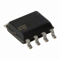
M93C66-WMN6 STMicroelectronics, M93C66-WMN6 Datasheet - Page 14

M93C66-WMN6
Manufacturer Part Number
M93C66-WMN6
Description
IC EEPROM 4KBIT 2MHZ 8SOIC
Manufacturer
STMicroelectronics
Datasheet
1.M93C46-WMN6TP.pdf
(36 pages)
Specifications of M93C66-WMN6
Format - Memory
EEPROMs - Serial
Memory Type
EEPROM
Memory Size
4K (512 x 8 or 256 x 16)
Speed
2MHz
Interface
Microwire, 3-Wire Serial
Voltage - Supply
2.5 V ~ 5.5 V
Operating Temperature
-40°C ~ 85°C
Package / Case
8-SOIC (3.9mm Width)
Lead Free Status / RoHS Status
Contains lead / RoHS non-compliant
Other names
497-1934-5
Available stocks
Company
Part Number
Manufacturer
Quantity
Price
Part Number:
M93C66-WMN6P
Manufacturer:
ST
Quantity:
20 000
Company:
Part Number:
M93C66-WMN6T
Manufacturer:
ST
Quantity:
881
Part Number:
M93C66-WMN6T
Manufacturer:
ST
Quantity:
20 000
Company:
Part Number:
M93C66-WMN6TP
Manufacturer:
ST
Quantity:
50 000
Part Number:
M93C66-WMN6TP
Manufacturer:
ST
Quantity:
20 000
Instructions
5.1
5.2
14/36
Read Data from Memory
The Read Data from Memory (READ) instruction outputs data on Serial Data Output (Q).
When the instruction is received, the op-code and address are decoded, and the data from
the memory is transferred to an output shift register. A dummy 0 bit is output first, followed
by the 8-bit byte or 16-bit word, with the most significant bit first. Output data changes are
triggered by the rising edge of Serial Clock (C). The M93Cx6 automatically increments the
internal address register and clocks out the next byte (or word) as long as the Chip Select
Input (S) is held High. In this case, the dummy 0 bit is not output between bytes (or words)
and a continuous stream of data can be read.
Write Enable and Write Disable
The Write Enable (WEN) instruction enables the future execution of erase or write
instructions, and the Write Disable (WDS) instruction disables it. When power is first
applied, the M93Cx6 initializes itself so that erase and write instructions are disabled. After
an Write Enable (WEN) instruction has been executed, erasing and writing remains enabled
until an Write Disable (WDS) instruction is executed, or until V
reset threshold voltage. To protect the memory contents from accidental corruption, it is
advisable to issue the Write Disable (WDS) instruction after every write cycle. The Read
Data from Memory (READ) instruction is not affected by the Write Enable (WEN) or Write
Disable (WDS) instructions.
Doc ID 4997 Rev 11
M93C86, M93C76, M93C66, M93C56, M93C46
CC
falls below the power-on


