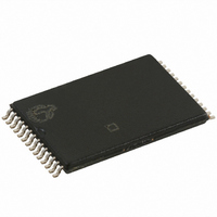
CY7C199C-12ZC Cypress Semiconductor Corp, CY7C199C-12ZC Datasheet

CY7C199C-12ZC
Specifications of CY7C199C-12ZC
Available stocks
Related parts for CY7C199C-12ZC
CY7C199C-12ZC Summary of contents
Page 1
... The device features an automatic power–down feature that significantly reduces power consumption when deselected. See the Truth Table in this datasheet for a complete description of read and write modes. The CY7C199C is available in 28 DIP, 28 SOJ, and 28 TSOP I package(s). Input Buffer RAM Array Power ...
Page 2
... Pin Layout and Specifications Document #: 38-05408 Rev DIP (6.9 x 35.6 x 3.5 mm) – P21 TSOP 13.4 x 1.2 mm) – Z28 CY7C199C I/O 7 I/O 6 I/O 5 I Page ...
Page 3
... Description 10, 21, 23, 11, 12, 13, 15, WE I/Ox Mode X High Z Deselect / Power-Down H Data Out Read L Data In Write H High Z Selected, outputs disabled CY7C199C I/O 7 I/O 6 I/O 5 I/O 4 I/O 3 DIP SOJ 10, 21, 23, 10, 11, 12, 13, 24, 25, 26 24, 25, 26 14, 15, 16, 17 11, 12, 13, 15, 18, 19, 20, 22, ...
Page 4
... CC IN GND Output Disabled CC GND Over the Operating Range (–20, –25) 3 Condition = Min –4 Min 8 CY7C199C Value –65 to +150 –55 to +125 –0.5 to +7.0 –0 0 > 2001 > 200 ) Voltage Range (V A 5.0V ± 10% 5.0V ± 10 Power Min. Max. Min. Max. – 2 ...
Page 5
... V 0.3V GND Output Disabled CC GND Conditions T = 25C MHz 5. 90 Rise Time 1 V/ns * including scope and jig capacitance CY7C199C Power Min Max Min = – – 75 – – – 30 – – 10 – – – 10 – L – 500 – – –5 +5 – ...
Page 6
... HZCE LZCE HZOE CY7C199C Nom 480 255 480 255 167 1.73 SOJ DIP 79 TBD 41.42 TBD Max Min Max Min – 20 – – 20 – – 3 – ...
Page 7
... Condition =2.0V – 0.3V – DATA RETENTION MODE OHA = CE. IL CY7C199C Min Max Min Max – 0 – 0 – 15 – 15 – 10 – 10 – 0 – – 10 – – 3 – 3 ALL Min Max 2.0 – – 150 ...
Page 8
... This cycle is WE controlled HIGH during write. 15. Data In/Out is high impedance 16. During this period the I/Os are in output state and input signals should not be applied. Document #: 38-05408 Rev ACE t DOE t LZOE t LZCE SCE HZOE Data-In Valid . IH CY7C199C HZOE Data Valid PWE HZCE High 50% Page ...
Page 9
... If CE goes HIGH simultaneously with WE going HIGH, the output remains in a high–impedance state. 20. The cycle is WE controlled, OE low. The minimum write cycle time is the sum of t Document #: 38-05408 Rev Data-In Valid SCE PWE t HZWE . IH and t HZWE CY7C199C t SCE Undefined Data-In Valid See Footnotes t LZWE . SD High Z Page ...
Page 10
... CY7C199C–15PC 15 ns CY7C199C–15VC 15 ns CY7C199C–15ZC 15 ns CY7C199C–15VI 15 ns CY7C199CL–15VC 15 ns CY7C199CL–15ZC 15 ns CY7C199CL–15VI 20 ns CY7C199C–20VC 20 ns CY7C199C–20ZI 25 ns CY7C199C–25PC Package Diagram Document #: 38-05408 Rev. *A Package Name Package Type V21 28 SOJ ( 3.5 mm) Z28 28 TSOP ...
Page 11
... The inclusion of Cypress Semiconductor products in life-support systems application implies that the manufacturer assumes all risk of such use and in doing so indemnifies Cypress Semiconductor against all charges. 28 SOJ (8 × 18 × 3.5 mm) – V21 28ÐLead(300ÐMil)Molded DIP P21 CY7C199C 51-85031-*B 51Ð85014Ð*B Page ...
Page 12
... Document History Page Document Title: CY7C199C 32K x 8 Static RAM Document Number: 38-05408 Issue REV. ECN No. Date ** 129233 09/11/03 *A 129697 09/15/03 Document #: 38-05408 Rev. *A Orig. of Change Description of Change HGK New Data Sheet KKV Minor change: Move Product Portfolio from page 4 to page 1 ...


