CY7C1019CV33-15ZXIT Cypress Semiconductor Corp, CY7C1019CV33-15ZXIT Datasheet
CY7C1019CV33-15ZXIT
Specifications of CY7C1019CV33-15ZXIT


Related parts for CY7C1019CV33-15ZXIT


CY7C1019CV33-15ZXIT Summary of contents
Page 1
... Document #: 38-05130 Rev Mbit (128K x 8) Static RAM Functional Description The CY7C1019CV33 is a high performance CMOS static RAM organized as 131,072 words by 8 bits. Easy memory expansion is provided by an active LOW Chip Enable (CE), an active LOW Output Enable (OE), and tristate drivers. This device has an automatic power down feature that significantly reduces power consumption when deselected ...
Page 2
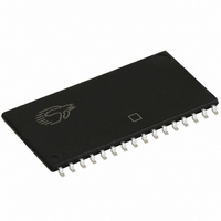
... Figure 1. 48-Ball VFBGA (Top View I I I Note 1. NC pins are not connected on the die. Document #: 38-05130 Rev. *G -10 (Industrial/ -12 (Industrial) Auto- Figure 2. 32-Pin SOJ/TSOP II (Top View I I/O I I/O I CY7C1019CV33 -15 (Industrial) Unit [ Page [+] Feedback ...
Page 3
... CC – 0.3V, CC – 0.3V, CC < 0.3V Test Conditions T = 25° MHz 5.0V CC CY7C1019CV33 Ambient V CC Temperature 3.3V ± 10% 0°C to +70°C 3.3V ± 10% –40°C to +85°C 3.3V ± 10% –40°C to +85°C –15 (Industrial) Unit Min Max Min Max ...
Page 4
... Auto-A) Min Max Min Figure 3. 3. Transition is measured ±500 mV from steady-state voltage. Figure is less than less than t , and t HZCE LZCE HZOE LZOE and t HZWE CY7C1019CV33 [4] High-Z characteristics: R 317Ω 3.3V 10% OUTPUT 5 pF (c) -15 (Industrial) Unit Max Min Max ...
Page 5
... If CE goes HIGH simultaneously with WE going HIGH, the output remains in a high impedance state. Document #: 38-05130 Rev. *G [11, 12] Figure 4. Read Cycle No OHA DOE DATA VALID 50 SCE t SCE PWE t SD DATA VALID CY7C1019CV33 DATA VALID [12, 13] t HZOE t HZCE HIGH IMPEDANCE t PD ICC 50% ISB [14, 15 Page [+] Feedback ...
Page 6
... During this period the I/Os are in the output state and input signals should not be applied. Document #: 38-05130 Rev SCE PWE t SD DATA VALID SCE PWE t SD DATA VALID Mode 7 Power Down Read Write Selected, Outputs Disabled CY7C1019CV33 [14, 15 [15 LZWE Power Standby ( Active ( Active ( Active ( Page [+] Feedback ...
Page 7
... Speed Ordering Code (ns) 10 CY7C1019CV33-10VC CY7C1019CV33-10ZXC CY7C1019CV33-10ZXI CY7C1019CV33-10ZXA 12 CY7C1019CV33-12VC CY7C1019CV33-12ZC CY7C1019CV33-12ZXC CY7C1019CV33-12VI CY7C1019CV33-12BVXI 15 CY7C1019CV33-15VC CY7C1019CV33-15VXC CY7C1019CV33-15ZXC CY7C1019CV33-15ZXI Package Diagrams Document #: 38-05130 Rev. *G Package Package Type Diagram 51-85033 32-pin 400-Mil Molded SOJ 51-85095 32-pin TSOP II (Pb-Free) 32-pin TSOP II (Pb-Free) 51-85095 32-pin TSOP II (Pb-Free) ...
Page 8
... Document #: 38-05130 Rev. *G Figure 10. 32-Pin TSOP II CY7C1019CV33 51-85095-** Page [+] Feedback ...
Page 9
... TOP VIEW A1 CORNER 6.00±0.10 SEATING PLANE C Document #: 38-05130 Rev. *G Figure 11. 48-Ball VFBGA ( mm) A CY7C1019CV33 BOTTOM VIEW A1 CORNER Ø0. Ø0. Ø0.30±0.05(48X 1.875 0.75 3.75 B 6.00±0.10 0.15(4X) 51-85150-*D Page [+] Feedback ...
Page 10
... Document History Page Document Title: CY7C1019CV33 1 Mbit (128K x 8) Static RAM Document Number: 38-05130 Submission REV. ECN NO. Date ** 109245 12/16/01 *A 113431 04/10/02 *B 115047 08/01/02 *C 119796 10/11/02 *D 123030 12/17/02 *E 419983 See ECN *F 493543 See ECN *G 2761448 09/09/2009 Sales, Solutions, and Legal Information Worldwide Sales and Design Support Cypress maintains a worldwide network of offices, solution centers, manufacturer’ ...