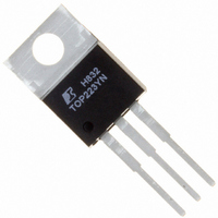
TOP223YN Power Integrations, TOP223YN Datasheet - Page 7

TOP223YN
Manufacturer Part Number
TOP223YN
Description
IC OFFLINE SWIT PWM OCP HV TO220
Manufacturer
Power Integrations
Series
TOPSwitch®-IIr
Type
Off Line Switcherr
Datasheet
1.TOP222GN-TL.pdf
(20 pages)
Specifications of TOP223YN
Output Isolation
Isolated
Frequency Range
90 ~ 110kHz
Voltage - Output
700V
Power (watts)
50W
Operating Temperature
-40°C ~ 150°C
Package / Case
TO-220-3
Output Voltage
5.7 V
Input / Supply Voltage (max)
265 VAC
Input / Supply Voltage (min)
85 VAC
Duty Cycle (max)
70 %
Switching Frequency
100 KHz
Supply Current
1.2 mA
Operating Temperature Range
- 40 C to + 150 C
Mounting Style
Through Hole
Supply Voltage
265VAC
No. Of Pins
3
No. Of Regulated Outputs
1
Filter Terminals
Through Hole
Output Voltage Max
700V
Rohs Compliant
Yes
Operating Temperature Max
150°C
Lead Free Status / RoHS Status
Lead free / RoHS Compliant
Other names
596-1158-5
TOP223YN
TOP223YN
Available stocks
Company
Part Number
Manufacturer
Quantity
Price
Company:
Part Number:
TOP223YN
Manufacturer:
PowerInt
Quantity:
3 250
Part Number:
TOP223YN
Manufacturer:
POWER
Quantity:
20 000
20 W Universal Supply using 8 Lead PDIP
Figure 8 shows a 12 V, 20 W secondary regulated flyback power
supply using the TOP224P in an eight lead PDIP package and
operating from universal 85 to 265 VAC input voltage. This
example demonstrates the advantage of the higher power 8 pin
leadframe used with the TOPSwitch-II family. This low cost
package transfers heat directly to the board through six source
pins, eliminating the heatsink and the associated cost. Efficiency
is typically 80% at low line input. Output voltage is directly
sensed by optocoupler U2 and Zener diode VR2. The output
voltage is determined by the Zener diode (VR2) voltage and the
voltage drops across the optocoupler (U2) LED and resistor R1.
Other output voltages are possible by adjusting the transformer
turns ratio and value of Zener diode VR2.
AC power is rectified and filtered by BR1 and C1 to create the
high voltage DC bus applied to the primary winding of T1. The
other side of the transformer primary is driven by the integrated
TOPSwitch-II high-voltage MOSFET. D1 and VR1 clamp
Figure 8. Schematic Diagram of a 20 W Universal Input TOPSwitch-II Power Supply using an 8 lead PDIP.
250 VAC
0.1 F
C6
J1
L
N
22 mH
L2
3.15 A
F1
400 V
BR1
400 V
47 F
C1
D
S
TOP224P
CONTROL
U1
47 F
C5
C
TOPSwitch-II
BYV26C
6.8
P6KE200
R3
D1
VR1
leading-edge voltage spikes caused by transformer leakage
inductance. The power secondary winding is rectified and
filtered by D2, C2, L1, and C3 to create the 12 V output voltage.
R2 and VR2 provide a slight pre-load on the 12 V output to
improve load regulation at light loads. The bias winding is
rectified and filtered by D3 and C4 to create a TOPSwitch bias
voltage. L2 and Y1-safety capacitor C7 attenuate common
mode emission currents caused by high voltage switching
waveforms on the DRAIN side of the primary winding and the
primary to secondary capacitance. Leakage inductance of L2
with C1 and C6 attenuates differential-mode emission currents
caused by the fundamental and harmonics of the trapezoidal or
triangular primary current waveform. C5 filters internal
MOSFET gate drive charge current spikes on the CONTROL
pin, determines the auto-restart frequency, and together with
R1 and R3, compensates the control loop.
T1
1N4148
0.1 F
D3
C4
MUR420
330 F
35 V
D2
C2
250 VAC
1 nF
PC817A
C7
Y1
U2
3.3 H
220 F
35 V
L1
C3
TOP221-227
100
1N5241B
R1
220
11 V
VR2
R2
PI-2019-033197
7/01
D
+12 V
RTN
7


